How to protect PCB?
By:PCBBUY 07/29/2021 17:24

As the core of electronics, PCBs and PCBAs (Printed Circuit Board Assembly) are responsible in implementing and contributing to the function achievement. If they fail to work in rugged environment, end products will become damaged or even a failure.
In this passage, we are talking about the methods to help PCBs’ better work in the harsh environment. Please check and read the content we prepare for you below to learn more professional information.
What are the environmental factors for PCB?
Environmental factors that normally affect a PCB are temperature, chemical attack, physical shock (vibration) and thermal shock; the trick is to decide which of these is likely to have the greatest impact upon your PCB and then concentrate on making an appropriate resin choice. Each of the three main resin types (epoxy, polyurethane and silicone) has its strong points, as well as weaknesses.
Silicone resins have the broadest continuous operating temperature range of any of the resin chemistries, so are a natural choice for both high and low temperature applications, as well as those subject to thermal shock. They also maintain their flexibility over this temperature range with very little sign of degradation over time. On the downside, silicones have poor adhesion on certain substrates and their chemical resistance is not as good as that provided by an epoxy resin.
As well as having excellent chemical resistance, epoxies provide good temperature performance. However, due to their rigid nature, epoxies are not so good at protecting against physical shock. Polyurethanes, on the other hand, have excellent moisture and physical shock resistance, but deliver poor high temperature performance. As a result, polyurethanes are best restricted to applications operating in the -40 to +120°C region. They do, however, provide similar levels of flexibility and better adhesion to many substrates compared with silicones – and at a lower cost.

How to protect PCB?
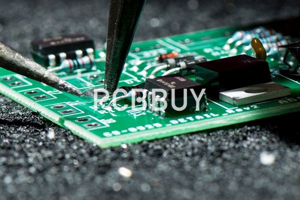
1. Conformal Coating
Conformal coating is quite a necessity whenever it comes to PCBs and PCBAs that have to work in harsh environment. It plays a protective role in stopping boards from erosion, moisture, dust etc. to finally prolong electronic products’ shelf life and ensure their performance and reliability.
Maintaining long-term and stable performance in nasty environment is quite a significant issue as far as electronic components and devices are concerned in both manufacturing and applications. Thus, it’s vital to make necessary protective measures in order to ensure electronic products to normally work in hostile environment.
As far as hostile environment is concerned, conformal coating should carry out some optimizations to better comply with extreme environment. Technical optimizations should be made on the following items that have been playing a role as protective measures: conformal coating shielding, electrostatic elimination and film thickness measurement.
Conformal Coating Shielding
Nowadays, PCB’s some parts with no need of conformal coating should be covered so that conformal coating won’t be sprayed on unnecessary sections (circuit board holder, potentiometer, switch, power resistor, connector for example) to stop signal abnormities from occurring. During the process of conformal coating implementation, masking tape is usually applied for conformal coating shielding. To comply with different shapes of different components in shielding, masking tape is cut into different shapes and dimensions. This method tends to bring forward quality concerns due to its downside including low efficiency, electrostatic generation, too much gel residue that is difficult to be eliminated.

Optimization measures
Conventional masking tape should be replaced by 3M shielding tape. Cutting method should be modified from knife cutting to the application of specialized cutting tool since the latter is capable of determining and cutting down different shapes based on the shape, volume and dimension of shielding covers. As long as unnecessary parts on board are covered by shielding covers, conformal coating won’t be sprayed on them.
Conformal Coating Film Thickness Measurement
Conformal coating is used on the surface of PCB, which is a thin, light and soft film that is only a couple of micrometers thick. This layer of film can effectively separate circuit board surface from the environment, stop circuitry from being eroded by chemicals, moisture and other pollutants. As a result, circuit board reliability will be dramatically improved with safety factors strengthened and shelf life guaranteed for in long term. Yet, the protective functions of conformal coating are hesitant to be implemented due to uneven coating. As a result, both PCB and end product will be failed, which is especially worse in harsh environment.
Optimization measures
Thickness measurement board should be made with metal materials and specialized instrument should be applied. In addition, before formal conformal coating spraying, test spraying should be first carried out and thickness is then measured. With all parameters determined, conformal coating can be done in volume so that thickness will be able to reach the standard.
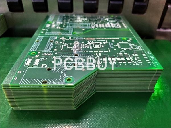
2. Board Cleaning
PCB cleaning aims to remove pollutants from board surface including gel residue, dust, oil, tiny particles and sweat in order to stop them causing erosion or other defects on components, printed wires and soldering points. The final purpose will be to improve the performance and reliability of electronic devices. Additionally, pollutant elimination can also help to improve combination between conformal coating and board surface and to protect products from being harmed by hostile environment during working and storage period. Cleaning optimizations should be implemented based on the analysis on post-solder cleanliness, surface ion residue and flux residue.
In the process of PCBA manufacturing, all kinds of pollutions are available in terms of physics, chemistry and mechanics, causing oxidation and erosion to board, which will then affect the reliability, electrical specification, and shelf life of end product. Leading pollutant sources contain pollutants on component leads, pollutants generated in assembly manufacturing process, flux pollutant and pollutants due to harsh working environment.
Nowadays, the biggest pollutant damaging circuit board lies in flux pollutant. Flux is active agent combined by organic acid and its containing organic acid salt and haloid, chloride or hydroxide all possibly become pollutants with corrosively. Of course, how to clean PCBs after surface mount soldering is not a concern of this article since how to optimize board cleaning procedures counts.
Optimization measures
First, severe damage should be analyzed including component lead breakage, printed wire breakage, plated through hole defect, reduced solderability and darkend soldering points caused by chemical, physical and mechanical pollutants. Then, the specific causes for abnormal signal transmission, partial heating and oxidation or even shorts should be analyzed as well in order to standards can be completed in terms of flux, solder paste and cleaning agent, which is the last step.
Well, the furthest distance in the world is not between PCB designer and PCB manufacturer but when PCB designer has got a fabulous idea yet it can’t be correctly understood by PCB manufacturer. However, if PCB designers prepare their design files by detail and show them in a way that is totally understood by PCB manufacturer and PCB manufacturer strives to cater exclusively to their design, the distance won’t be long.
Industry Category


