How to reduce electromagnetic interference in PCB?
By:PCBBUY 06/07/2021 17:52
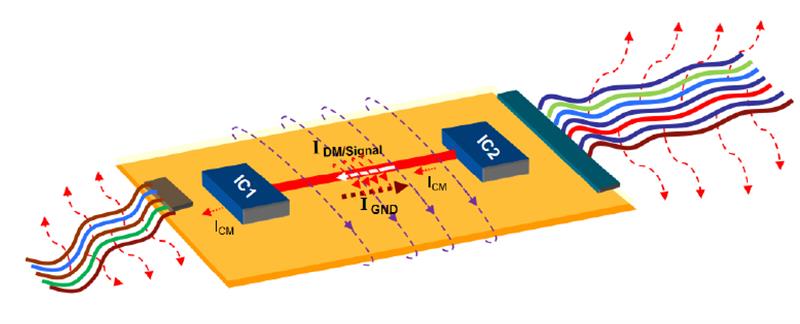
During the PCB manufacturing process, electromagnetic interference will consistently plague PCB designers. So the testing of electromagnetic interference is extremely important to designers so that they could monitor electromagnetic compatibility and interference.
Electromagnetic compatibility, or EMC, involves the generation, propagation and reception of electromagnetic energy, generally through poor design. Electromagnetic interference, or EMI, refers to the unwanted and damaging effects of EMC, as well as electromagnetic interference from environmental sources. Too much EMI can result in a defective or damaged product. Any PCB designer should follow EMC design rules to minimize the amount and effects of EMI.
Please check and read the content we provide and get to learn how to reduce electromagnetic interference in PCB manufacturing.

Why to avoid electromagnetic interference?
Sources of electromagnetic interference are all around us, and we can categorize them in several ways:
Source
Human-made EMI arises from electronic circuits. Naturally occurring EMI, on the other hand, can arise from environmental factors like cosmic noise and lightning.
Duration
Continuous interference is an EMI source that emits a constant signal, which most often appears as background noise. Impulse interference is intermittent, usually caused by switching systems, lightning and other non-constant sources.
Bandwidth
Narrowband signals like those used by radio can encounter interference from oscillators and transmitters, though these sources only affect certain parts of the spectrum intermittently. Broadband interference affects high-data signals like TV and can come from many sources, including arc welders and solar noise.
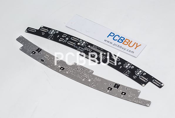
Whether human-made or environmental, EMI can be both costly and dangerous. It can disrupt communication channels and sensitive devices. EMI is a notable concern in the medical field, where wirelesses device usage is on the rise. Unfortunately, EMI can affect the functionality of medical equipment like ventilators, ECG monitors, cardiac monitors and defibrillators. In other industries, EMI can disrupt sensors and navigational systems. The result in all cases is a disturbance of equipment that may be responsible for the health and safety of its users.
However, the most common source of EMI — and the most problematic source for designers — is internal. Poor PCB design can result in incompatible signals interfering with one another on the board. This interference can ultimately cause the board to fail. Designers must ensure that interference is kept to a minimum and any signals let off are compatible so as not to result in interference.
How to prevent electromagnetic interference in PCB?
These essential design principles can help prevent and fix these electromagnetic problems in a printed circuit board design.
1. Ground Plane
Designing a PCB’s ground plane is the most significant step, and it’s crucial for reducing EMI. The ground plane is your first line of defense against EMI since all circuits require a ground to work. Some common best practices for ground design to reduce EMI include:
Maximize ground area: Increase the ground area as much as possible within the PCB. Signals can disperse more easily with more area, reducing emissions, cross-talk and noise. If the ground plane is too small, you could possibly add another layer and create a multi-layer PCB. This design solution provides more options for handling high-speed traces.
Use solid planes: Especially in multi-layer PCBs, a solid ground plane is an ideal option. Copper-thieving and hashed ground planes usually result in higher impedance levels. Solid ground planes, on the other hand, provide lower levels.
Connect each component: Connect every part to a ground plane or point. The ground plane acts as a neutralizing agent for board design, and floating components don’t fully make use of this.
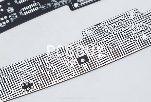
Be careful with split planes: Highly intricate PCB designs often include numerous regulated voltages, which should each have their own ground planes. Too many ground planes, however, increases fabrication cost. This issue is usually circumvented through the use of split planes, which create multiple ground sections on a single layer. However, designers should always use split planes carefully. Ensure you have a good reason to use a split plane and, if using one, make sure they are only connected at a single point. Multiple ground connections in a split-ground PCB can create loops, resulting in an antenna that radiates EMI.
Connect bypass or decoupling capacitors: If the design includes bypass or decoupling capacitors, connect them to the ground plane. This act helps lessen the return current by reducing the size of the loop.
Minimize signal length: The length of traces is important since the amount of time a signal takes to get to and from a source must be compatible. Otherwise, it can radiate EMI. Keep trace lengths are as short as possible and are about equal in length.

2. Trace Layout
Traces are especially important for board design. Proper trace usage ensures properly propagated current. However, many problems can arise if traces are not arranged according to top EMC design rules.
Traces are essentially conductive paths that contain flowing electrons while the circuit is active. Thus, these traces are one mistake away from creating a radiating antenna. A simple bend or cross can result in PCB electromagnetic interference.
Some of the best rules for trace layout in PCB design include:
Avoid right angles: Avoid angles of 45 degrees to 90 degrees for vias, traces and other parts. Capacitance increases as traces reach angles over 45 degrees. As a result, the characteristic impedance changes will lead to reflection. This reflection results in EMI. You can avoid this problem by rounding out traces that need to turn a corner or routing them through two or more angles of 45 degrees or less.
Keep signals separate: Keep high-speed traces separate from low-speed signals and analog signals separate from digital ones. Close proximity can result in interference.
Shorten return paths: Keep return current paths as short as possible, and route them along paths of least resistance. Return paths should be about the same length as transmit traces or shorter.
Mind spacing: Two high-speed signals running in parallel create EMI through cross-talk, in which one trace is the “aggressor” and the other is the “victim.” The aggressor influences the victim trace through inductive and capacitive coupling, creating forward and backward current in the victim trace. You can minimize cross-talk by keeping a minimum spacing between traces. Generally, separate traces by twice the trace width. For example, if the traces are five-thousandths of an inch wide, keep a minimum distance of ten-thousandths of an inch or more between two parallel traces.
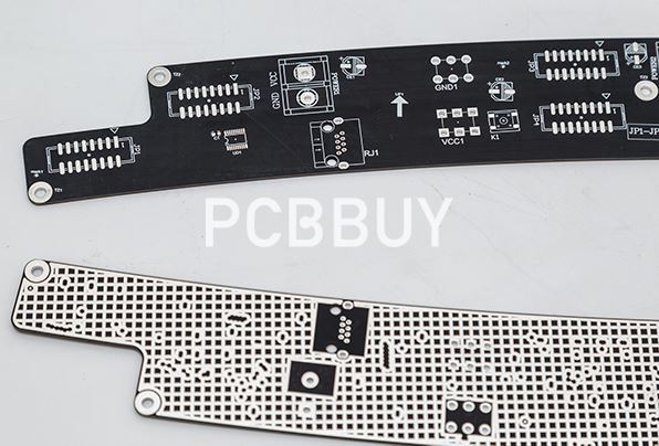
Use vias carefully: Vias are necessary in PCB design because they let you take advantage of multiple layers in your boards when routing. However, designers must be careful when using them. Vias add their own inductance and capacitance effects to the mix, potentially resulting in reflections due to changes in characteristic impedance. Vias also increase trace length, which needs to be matched. When possible, avoid using vias for differential traces. If this is impossible, however, use them in both traces to compensate for the delay.
3. Component Arrangement
Electronic components are the building blocks of an electronic circuit. However, arranging them improperly can cause several EMI issues. When designing a PCB, be mindful of each piece’s EMI impact. Some best practices for component layout in PCB design include the following:
Separate analog and digital parts: As with traces, always separate analog and digital circuits and components. Placing analog and digital circuits in close proximity can result in cross-talk, among other issues. To avoid this, use shielding, multiple layers and separate grounds to place analog and digital signals as far away from each other as possible. Generally, it’s best to keep analog and digital signals on separate grounds altogether.
Separate analog and high-speed pieces: Analog circuits carry high current, which can cause problems for high-speed traces and switching signals. Keep these away from one another and guard analog circuits with ground signal. On multi-layer PCBs, route analog traces so that a ground plane exists between the analog circuit and the switching or high-speed signals.
Be careful with high-speed components: The faster and smaller the component is, the greater the amount of EMI it likely produces. You can combat this natural EMI through shielding and filtering, though it’s also a good idea to separate these components from others in the board design. Another measure to take is to keep high-speed signals and clocks as short as possible and adjacent to the ground plane. These measures help keep cross-talk, noise and radiation levels in check and within the acceptable level limits.
4. EMI Shielding
Some components will produce EMI no matter what design rules you follow — especially small, high-speed parts. Fortunately, shielding and filtering can keep this EMI’s effects to a minimum. Some shielding and filtering options include the following:
Component and board shielding: Physical shields are metallic packages that encapsulate all or part of a board. Their goal is to keep EMI from entering the board’s circuitry, though the specific methods vary based on the EMI’s source. For EMI that comes from within the system, component shields may be used to encase a specific component that produces EMI — thus connecting to ground, reducing the antenna loop size and absorbing EMI. Other shields may encase the entire board to protect against EMI from outside sources. A Faraday Cage, for example, is a thick protective enclosure designed to block RF waves. These devices are usually made of metal or conductive foam.
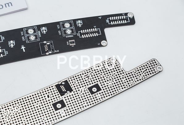
Low-pass filtering: Sometimes, a PCB can include low pass filters to eliminate high-frequency noise from components. These filters suppress the noise from these part, allowing the current to continue on the return path without interference.
Cable shielding: Cables that carry analog and digital currents create the greatest amount of EMI issues. They produce these issues by producing parasitic capacitance and inductance — a particular problem for high-frequency signals. Fortunately, shielding these cables and connecting them to ground at the front and back helps cancels out EMI interference.
Industry Category


