How to repair broken PCB traces?
By:PCBBUY 05/24/2021 18:26

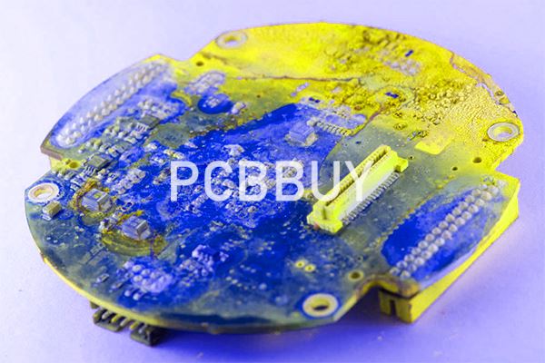
Printed circuit boards are easily damaged. All it takes to crack a trace is a little rough handling during installation or removal. It doesn't even have to be deliberate roughness, some of the plug-in boards just don't want to enter or exit their sockets without the use of a little force. Apply a little bit too much heat for a little too long during the installing or removal of components and the copper trace will lift free of the board's substrate. Finding a microscopic crack in the trace is the most part of making the repair.
In this passage, we will talk about the methods of how to repair the broken PCB traces and if you are curious about it, please check the content we provide below.
Why We Have to Repair PCB?
Why bother at all with learning component-level PCB board repairs for PCBs? Don’t we live in a throwaway culture in which it’s OK to toss electronics in the landfill at the first sign of trouble?
This is the first reason why it makes so much sense to learn everything that you can about repairing PCBs. People who have a passion for electronics, and for upcycling or getting the maximum lifespan out of something, can find a lot of satisfaction in the process of locating damaged tracks or identifying failed board components, replacing them, and restoring a PCB product.
On the hobbyist as well as the professional side of things, an understanding of how PCBs function and how to restore them is essential if you want to learn how to build and maintain your own projects and systems, such as the following:
Garage door openers
Home theater systems
Speed controllers for powered tools
Televisions
Computers
Electrical engineers have even more motivation for pursuing a masterful knowledge of this fundamental skill. Both the consumer and commercial landscape rely on ever more sophisticated electronic devices, most of which require PCBs. Knowing how to diagnose problems with these boards and repair or replace failed components means that a technician can perform troubleshooting on a wide range of computerized assets and internet of things (IoT) devices.
How to Repair PCB Step by Step?
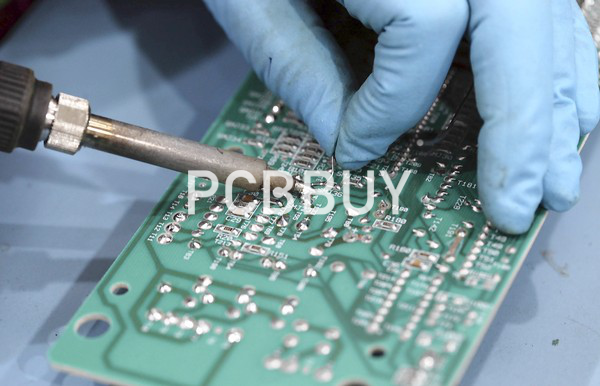
Step 1: Remove the damaged pad or component. First, secure the PCB to your work surface so that it doesn’t move around while you’re working on it. It’s best to use tape.
Sometimes, diagnosing a damaged and inoperable PCB requires the application of an oscilloscope to probe the signal strengths and waveforms at various points to test for continuity of the circuit across the board. Other times, it’s just a matter of looking for a burned area that indicates that a failed component or a pad or trace needs to be replaced and rejoined to the existing track on the PCB.
If you find that one of the components on your PCB isn’t functioning the way that it should, there’s a simple process for removing and replacing it:
Grab the hot air gun and turn it on. Hold it no fewer than 6 inches from the failed component.
After a few seconds, take a pair of tweezers and attempt to lift the component away. If it doesn’t come, continue to apply heat for a few more seconds and then try again.
If a PCB pad has been damaged by heat, it’s best to use a sharp knife to carefully remove it. Your priority is to limit the amount of damage that you do to the track and the other nearby features while still freeing the board from any residue.
Step 2: Clean the track and remove solder. Once you’ve removed the damaged pad, continue using your sharp knife to remove the existing solder. If you’re not comfortable using a knife for this relatively delicate part of the operation, a sharp-pointed screwdriver or sandpaper with a very fine grit will work, too.
No matter which tool you prefer, the result should be a fully exposed track, free of existing solder, which looks shiny and clean.
Step 3: Place your copper tape over the track. After you’ve removed the damaged track and cleaned off the area, it’s time to place your adhesive copper tape over the top of the area that you’re working with.
Your tape should overlap with the existing track and cover the existing through-hole and a portion of the area surrounding it.
Step 4: Solder the joints. From here, it’s a matter of carefully soldering the joints where the new copper tape joins with the existing track on your restored PCB. Here are a few tips and warnings about this part of the process:
Copper tape melts quickly at soldering temperatures, so don’t begin until you’re certain that you can finish this part of the process in one go.
Use as little heat as possible and work deliberately, but quickly, to reduce the amount of heat applied.
Step 5: Restore the PCB through-hole. Find a hard implement with a rounded-off end, like a pen or another simple tool. Press down on the area that you’ve just soldered and rub firmly to ensure that the copper tape is securely affixed to the entire pad area. The adhesive should still be tacky after you’ve applied heat to the area.
With this technique, you’ll be able to identify where the through-hole is, which you can then pierce with a paper clip or another similar implement.
Step 6: Place and solder your component. If you’ve followed these steps so far, you should have a PCB that’s been restored to functionality and is ready to receive your component of choice.
From here, soldering the components should be a familiar process. However, you’ll want to keep your application of heat as brief as possible. The new joint that you’ve formed between the freshly affixed copper tape/pad and the track may be somewhat fragile.
Step 7: Trim excess tape from the repaired area. Using your scissors or craft knife, carefully cut the adhesive copper tape down to size to finish the repair. It’s important to note that the joint that you’ve just repaired may restore your PCB to functionality, but the pad, track, and joint will never be as structurally sound as the original board. Nevertheless, you’ve taken something that many others would discard as junk and given it a new lease on life.
Industry Category


