How to reverse engineer PCB?
By:PCBBUY 06/02/2021 17:34

PCB reverse engineering is a multilayered process that includes targeted PCB research, reverse analysis and PCB design technology reproduction. The process is also used to identify and obtain the design of a product’s functional and structural characteristics, as well as the processing flow. With this information, a company can produce products with similar functions and abilities — though businesses will make sure they’re not reproducing an exact replica of a reverse-engineered PCB.
To get into the knowledge of reverse engineer, you may know the working principles of PCB and know how to repair and produce better products than competitor. Let’s check the content below to learn more information.
Why reverse engineer a PCB?
There are several advantages of reverse engineering PCBs — many companies use these devices for various purposes. Reverse engineering can also help you produce more effective or less costly versions of a competitor’s PCBs.
Learn more about the advantages of reverse engineering PCBs below:
-Maintain crucial PCBs
-Get information on PCBs without documentation
-Reduce your reliance on experts
-Identify weaknesses in a competitor’s designs
-Produce less costly PCBs
How to reverse engineer a PCB?
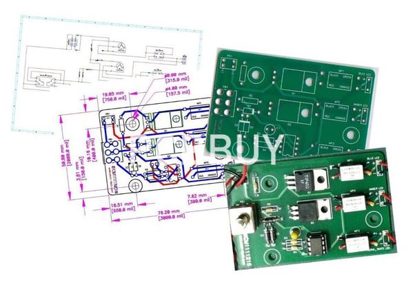
Reverse engineering circuit boards can be a long process, but it’s well worth the payout. There are a few primary stages of reverse engineering PCBs that anyone who attempts to do it should follow. These steps include creating initial drawings, scans or photographs of PCBs that are then uploaded to the appropriate reverse-engineering software and programs. Once uploaded, users have to build the PCB’s layout and use that layout to create schematics.
After conducting these main steps, you’ll know exactly how a PCB works, which can assist you with whatever goal you have. If you want to learn more about this process, check out an overview of how to reverse engineer PCBs below:
1. Draw, Scan or Photograph the PCB for Image Prep
The first step to reverse engineering a PCB is drawing, scanning or taking a photograph of the PCB. If you take pictures of it, ensure you photograph both sides of the PCB. It’s also crucial to take pictures of it on a dark background. Since PCBs may have holes in them, you don’t want any background visible through these holes, as lighter backgrounds might look like copper. A dark background prevents any confusion about the PCB’s construction.

Another necessary step for properly photographing PCBs is to use a high-quality camera that can capture every detail. Digital cameras or smartphones usually suffice for this step. For simpler PCBs, you may be able to draw the layout on a piece of graph paper.
2. Upload the Image
Once you’ve taken the pictures, you can then upload them to your reverse engineering program. Before you upload the imagery, manually crop the image so the photo only shows the PCB. There are multiple programs available online to help you edit any photos or scans and manipulate key PCB features.
For instance, you may want to use GIMP or Inkscape — both platforms are open-source, free graphics editors. Inkscape is a vector graphic editor. Dia is another free, open-source software solution for general-purpose diagramming. You may also want to consider using AutoTrace, a program that converts bitmap to vector graphics.
All these programs can be helpful in the schematic development and layout building processes. Once you complete the schematic development and layout building processes, you may still require CAD software to get more detailed results.

3. Construct the Layout
After uploading your images to your chosen reverse-engineering PCB program, you’ll then need to build a 3D layout of the PCB. A PCB’s layout shows how the system’s electromagnetic field distribution is arranged and how the circuits behave. It also represents other parts of a PCB that can’t be shown in a schematic, such as components, conductive elements, the arrangement of traces and each layer’s planes.
The following are some primary editing steps used on each side of the PCB to build the layout:
“Paint” holes and solder pads: Before transferring the PCB, you’ll need to “paint” the solder pads and holes to ensure you don’t lose them. You can achieve this by swapping channels, as these can improve the holes’ visibility.
Remove PCB trackpads: Users who run their PCBs through AutoTrace will need to get rid of any PCB trackpads before using the software. These PCB trackpads can convert to loops in the program, so you should remove them to maintain accuracy.
Mark free holes: Multilayer boards often have holes or areas on them that don’t connect to anything else or connect to the PCB’s inner layers. You should mark these holes during the editing stage so you can identify them.
Adjust saturation and layers: To increase visibility on painted PCBs, adjust the saturation and layers.
Clean tracks: Before converting the PCB imagery in a program like AutoTrace, clean any tracks.
Desaturate and invert image: To desaturate the image, apply grayscale to it. Once you complete this, you’ll invert the image so the PCB’s lines become dark and are displayed on a white background. This desaturation process is crucial to obtaining a more accurate AutoTrace transfer, as it clears out any white or gray colors.
Repeat process on the other side: To craft a full layout, you’ll need to conduct the above editing steps on the other side of the PCB. If you don’t repeat the processes for the other side of the PCB, you won’t be able to produce the dual-sided schematic needed to reverse engineer a circuit board.
4. Create Schematics
The next step is to derive the PCB’s schematic. When you derive a PCB’s schematic diagram, you can see every circuit and all of the board’s components. The diagram will usually take the form of a 2D CAD assembly drawing. This 2D representation of the schematics helps an engineer see how different components connect and what their functionalities are. All of this information is crucial when you’re attempting to repair or reproduce a PCB.
To create a schematic, you can use a program like AutoTrace or a PCB layout CAD program tool like Target 3001!. This step is often relatively easier than the layout stage, as you’ll have already finished any drawing or photo editing needs.
After creating the schematics, you’ll need to combine both sides of the PCB, arrange the tracks and label the components with symbols. By labeling and arranging tracks, you’ll find it easier to interpret the schematic. If you’re reverse engineering a PCB so you can repair it, you can go through the schematic and use it to troubleshoot the PCB. This troubleshooting process often involves replacing any needed lines and inspecting key components.
Industry Category


