How to use test points on PCB?
By:PCBBUY 05/12/2021 17:44

As a design for test approach, test points streamline the PCB testing process. These design elements will enable you to verify your PCB’s function during development. By creating a PCB with test points, you can improve processes that happen in later stages of production.
What is a PCB test point?
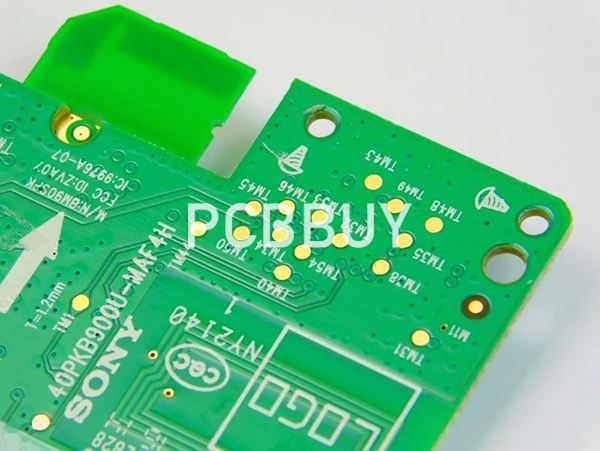
A PCB test point is a small wire loop used for test probes on a PCB that contains surface-mount parts. During production, they enable the user to inject test signals or monitor the board’s circuitry. Test points come in a variety of materials, sizes and colors.
With a test point, we could create an access area for your test probe. Many of these probes have J-hooks designed for older PCB styles that included leads. A PCB test point provides a place for the J-hook or has a sharp pointed end that touches a conductor on the board. Most surface-mount test points feature a phosphor bronze alloy, but they can also have more affordable silver plate coatings.
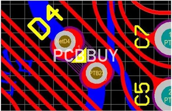
Very simply, a PCB test point is an electrical pad or via that can be probed during an ICT. These points are used to monitor voltage, current, and/or signal behavior in specific circuits. They can also be used to inject signals into a circuit. A pad on an existing component or a specific via in an existing layout can be assigned as a test point. The other option is to create custom test points in your schematic and import them into your layout during capture.
How to use test point on PCB?
To function as a PCB test point, the test point must be an exposed metal spot on an exterior layer of the board that is connected to a net. This will allow the probes of the automated test equipment to make contact with it to conduct the test. As the test probe tips are available in a variety of shapes for different testing surfaces, each test point on the board can be matched up with a probe that is best suited for it.
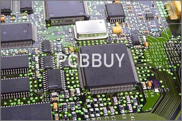
Not only is the board tested to verify that it will function as designed but also that it has been assembled correctly and is ready to be put into service. To facilitate this testing, printed circuit boards are designed with small metal contacts called test points. Here is a brief overview of what PCB test points are and how you as a designer should work with them.
To verify the integrity of the component assembly process, a completed printed circuit board will go through an automated test cycle. This is designed to find component pins that are not connected to the board with a good solder joint and will use a system of probes to contact the test points designed into the board. There are two different systems that are generally used for this testing:
ICT
This is a system that is designed to test all of the nets on the circuit board simultaneously. To do this, ICT employs the use of a test fixture that is loaded with probes to contact the test points on the board. The fixture will have one probe for each test point on the board, which enables the testing to be conducted very quickly. These test fixtures are usually configured to test the bottom of the board, but they can also test the top or both sides of the board at the same time.
ICT is a system that uses a test fixture that is prepared exclusively for a specific circuit board design as well as accompanying software that will be run on the test system. The fixture and software are created using the test point locations and other design data generated by the CAD database, and a probe will be used for each net on the design. While the main purpose of ICT is to verify the assembly of the board by testing each net for a good connection to its associated part pin, it can also be used to test the functionality of the board.
ICT test fixtures and software are expensive and time-consuming to develop. The test fixtures are complex with thousands of probes in them and changes to a fixture for board revisions can also be very expensive. Once developed, though, the in-circuit test will test large amounts of circuit boards very quickly. For mass production, the benefits of speed and functional testing quickly offset the development time and costs of ICT.
Flying probe
This system differs from ICT in that it only uses between two and six probes to conduct all of the tests on the board. As the name would suggest, these probes fly around the board contacting each specific test point sequentially that they are programmed to test. Due to the more individualistic nature of the testing, the flying probe takes a lot longer to test a board than an ICT will. Flying probes also aren’t able to conduct any functional testing of the board due to the minimum amount of test points that are being probed at one time.

The disadvantage of the flying probe is that it is very slow. Where ICT can test all of the points on the board almost instantaneously, the flying probe system has to maneuver its probes around to each individual test point. On a large board, this can take a very long time, and the ability to do functional testing is eliminated. However, for prototypes or low volume production runs, using the flying probe for testing can be very advantageous.
Wanna know PCB knowledge? Check and read for more.
Industry Category


