IPC Component Spacing Guidelines
By:PCBBUY 09/04/2021 09:47

The IPC component spacing guidelines exist for two reasons: to prevent component overlap that could cause physical damage and to prevent electrical interference that could cause performance problems. Of the two, physical overlaps are a simpler problem to correct.
If you are going to learn the professional knowledge about IPC component spacing, please follow us and read the content we prepare below for more information.
What is the importance of IPC component spacing?
First, let’s review what some of the assembly problems are for PCB manufacturers when minimum spacing requirements aren’t met:
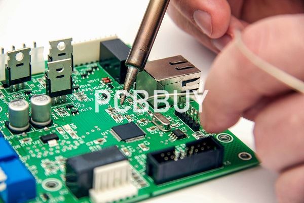
· Component installation: Although automated placement equipment is extremely accurate, those systems still need enough room to operate in. Parts that aren’t candidates for machine placement, will need even more room for technicians to be able to work with them.
· Soldering: For boards that are to be wave soldered, the spacing between parts is extremely important to prevent shadowing of smaller parts by larger. As with component installation, those that are to be manually soldered need enough room for the technician to be able to work with.
· Test: There must be enough clearance between test points and components to allow access for the probes of the test fixture. There also needs to be proper clearance around the perimeter of the board for the test fixture outline.
· Access: Printed circuit boards usually have connectors, switches, and other interfaces that require access for technicians. There needs to be enough clearance to fit fingers and tools in for a test, debug, rework, and normal operations.
What is the purpose of IPC component spacing?
The IPC component spacing guidelines are a third check on these potential physical problems. As long as designers follow the spacing guidelines, there should not be physical overlaps of components except in special circumstances that require additional engineering and development.

Component spacing guidelines also manage negative space—the places where components are not present. Negative space on a PCB can be just as important as the regions where components exist, and this space is particularly important when preventing electrical interference. If conductive traces or circuits are too close together, unintentional connections may form between them as electrons jump between circuits.
These unexpected connections reduce the strength of signals traveling through some regions of the PCB and can increase the amount of power flowing through other areas. Reductions in power can cause shorts or failures, while surges in power can cause physical damage or overloads.
What are the considerations of IPC component spacing?
There’s a common saying that goes something like this – PCB design is 90% placement and 10% routing. This is entirely accurate. Taking the time to precisely place your components will make your life a whole lot easier when it comes time to route everything, while also giving your board its best electrical performance. But what happen if you just slap your components down without care?
IPC component spacing guidelines help designers create circuits that minimize interference while still making the best possible use of space. There is no minimum or maximum size for a circuit defined in the standard, so the guidelines are applicable to PCBs of any size. Instead, the guidelines recommend that designers decide upon the proper size for circuits and traces based on the amount of current they should carry, as well as their thermal tolerance.
· Hours Wasted. You’ll likely create a nightmare for yourself when you find out that some of your parts don’t even have enough space to be routed because you packed them too close together. The worst component placement jobs can lead to an entire board that needs to be started again from scratch.
· Busted Boards. Let’s say you do manage to place down some components and traces and ship your files off to your manufacturer. Next thing you know you might get a board back, that doesn’t work because your parts weren’t soldered correctly (more on this later).
· Ugly Aesthetics. Let’s face it, as engineers we love symmetry and precision, and there’s nothing more unsettling than seeing a board that wasn’t given some proper love and care during its component placement. It’s just plain lazy.

Many sizes of PCB boards are standardized, ranging from a few millimeters long to a third of a meter. In all PCBs, conductor leads should be as short as possible. Leads can be theoretically placed on a PCB at any angle and in any orientation, but unusual angles can make these leads more difficult to model computationally.
The IPC recommends that leads be placed parallel to each other, perpendicular to each other, or at 45-degree angles to each other. It is common for a single PCB to have leads running in different directions, but leads should never overlap. Overlapping leads would be a violation of component spacing guidelines and could cause a lot of interference.
Industry Category


