Impedance Control in PCB Manufacturing
By:PCBBUY 08/13/2025 16:57
Introduction to Impedance Control in PCB
In today’s high-speed and high-frequency electronics, impedance control in PCB manufacturing has become a fundamental requirement for ensuring signal integrity and reliable product performance. As circuits operate at faster speeds, even small variations in impedance can cause signal distortion, reflection, and data loss.
At PCBBUY, we specialize in delivering high-precision impedance-controlled PCBs with tight manufacturing tolerances and state-of-the-art testing capabilities. Our expertise ensures that every board we produce meets the exact impedance requirements defined by your design specifications.
What is Impedance Control in PCB?
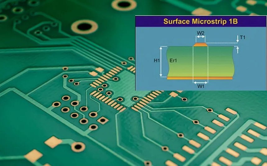
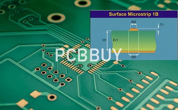
Impedance control refers to the precise regulation of the electrical resistance (in Ohms) that a signal encounters as it travels through PCB traces. This characteristic impedance is determined by several factors, including:
-
Dielectric constant (Dk) of the PCB material
-
Copper thickness
-
Trace width and spacing
-
PCB stack-up design
Controlled impedance ensures that signals pass through the PCB without unwanted reflection or distortion—critical in high-speed applications such as telecommunications, automotive radar, and advanced computing.
The Science Behind Impedance Control
For a given PCB trace, the target impedance value might be 50Ω (single-ended) or 100Ω (differential). However, real-world manufacturing tolerances can cause slight variations.
At PCBBUY, our minimum impedance tolerance is ±10%, meaning:
-
If the target impedance is 50Ω, the actual measured impedance will be between 45Ω and 55Ω.
Formula:
Lower Limit = T − (T × 10%) = 50 − (50 × 0.1) = 45Ω
Upper Limit = T + (T × 10%) = 50 + (50 × 0.1) = 55Ω
This high-precision tolerance ensures that your circuit design functions exactly as intended.

PCBBUY’s Impedance Control in PCB Manufacturing Capabilities
We provide a complete solution for impedance-controlled boards, from engineering consultation to final testing:
1. Engineering Expertise
-
In-house design review (DFM) to validate stack-up and impedance values
-
Simulation software to verify target impedance before production
2. Stack-Up and Material Selection
-
High-performance FR4, Rogers, and hybrid laminates
-
Consistent dielectric properties for stable impedance
3. Precision Fabrication
-
Advanced etching and plating processes to maintain exact trace widths
-
Layer-to-layer registration accuracy for multi-layer boards
4. Tight Tolerance Control
-
±10% minimum impedance tolerance
-
Process adjustments in real time to maintain stability
5. Advanced Testing
-
TDR (Time Domain Reflectometry) measurement for every production batch
-
Full impedance report provided with each shipment
Manufacturing Process of Impedance Controlled PCBs at PCBBUY
-
Customer Design Review – Our engineering team reviews your Gerber files and impedance requirements.
-
Stack-Up Confirmation – Material and copper thickness are finalized to meet impedance targets.
-
Simulation & Calculation – We run pre-production simulations to verify results.
-
Trace Processing – Precision etching ensures consistent trace geometry.
-
Lamination & Pressing – Stack-up layers are bonded under controlled conditions.
-
Impedance Testing – TDR tests are conducted, and results are matched with specifications.
-
Final Inspection & Delivery – Boards are packaged with full quality reports.
Advantages of Choosing PCBBUY for Impedance Control in PCB
-
High Accuracy – ±10% impedance tolerance for consistent performance
-
Material Flexibility – FR4, Rogers, PTFE, and mixed dielectric solutions
-
Custom Solutions – Single-ended and differential impedance designs supported
-
Speed & Reliability – Capable of both prototype and mass production with short lead times
-
Global Quality Standards – IPC, ISO, and RoHS compliance

Applications of Impedance Controlled PCBs
-
5G base stations and network infrastructure
-
High-speed data centers and servers
-
Automotive radar and ADAS systems
-
RF modules and microwave antennas
-
Medical imaging and diagnostic equipment
Common Challenges in Impedance Control and PCBBUY Solutions
|
Challenge |
Impact |
PCBBUY Solution |
|
Material variation |
Changes dielectric constant |
Strict supplier selection, batch testing |
|
Copper thickness deviation |
Alters impedance |
Automated plating control |
|
Etching width tolerance |
Affects trace geometry |
Laser direct imaging (LDI) and precision etching |
|
Stack-up misalignment |
Differential pair mismatch |
High-accuracy layer registration |
Conclusion
In the rapidly evolving electronics industry, impedance control in PCB manufacturing is no longer optional—it’s essential. With PCBBUY’s advanced engineering capabilities, tight process control, and rigorous testing, we ensure your high-speed designs perform flawlessly.
Whether you need prototypes or large-scale production, PCBBUY is your trusted partner for impedance-controlled PCB solutions. Contact us today to discuss your requirements and experience the precision of PCBBUY manufacturing.
FAQ – Impedance Control in PCB
Q1: What is the standard impedance tolerance at PCBBUY?
A1: Our minimum tolerance is ±10%, verified by TDR testing.
Q2: Can PCBBUY manufacture both single-ended and differential impedance PCBs?
A2: Yes, we support both 50Ω single-ended and 90–100Ω differential impedance designs.
Q3: Does impedance control increase PCB cost?
A3: There is a small additional cost due to tighter process control and testing, but it ensures long-term reliability.
Q4: Which industries most require impedance-controlled boards?
A4: Telecommunications, automotive electronics, medical devices, aerospace, and data centers.
Industry Category


