Low-Cost High Layer Count PCB Fabrication
By:PCBBUY 10/24/2026 15:49
Introduction
High-layer-count PCBs enable complex routing, stable power distribution, and improved signal integrity in demanding electronic systems. However, increasing the number of layers also adds material consumption, lamination steps, drilling requirements, and manufacturing complexity.
The goal of low-cost high layer count PCB fabrication is not simply to choose the cheapest materials. It is to optimize the stackup, via structure, panel utilization, and manufacturing process while maintaining the electrical, thermal, and reliability requirements of the finished board.
For automotive electronics, industrial control, power systems, energy storage, new-energy equipment, and embodied robotics, early design-for-manufacturing (DFM) review can help reduce unnecessary cost and avoid production delays.
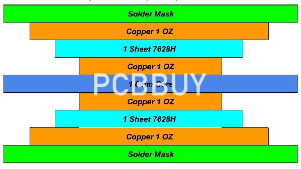
1. Optimize the Layer Stackup Before Fabrication
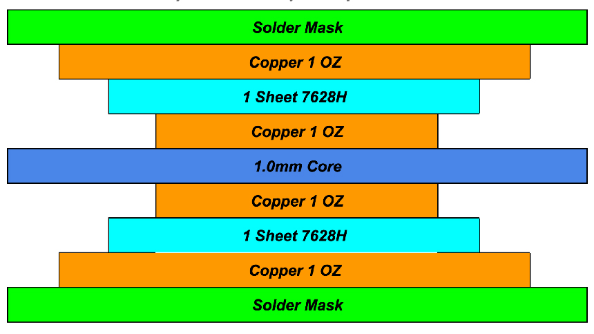
Each additional copper layer adds material and processing requirements. An unnecessarily complex stackup can increase fabrication cost without delivering a meaningful improvement in performance.
Before finalizing the design, engineers should review whether all signal, ground, and power layers are necessary. A balanced stackup can support more consistent lamination behavior, while suitable reference planes help maintain signal integrity and power distribution.
However, reducing layer count should not compromise routing capacity, impedance control, current-carrying capability, or thermal performance. For power electronics and battery management systems, copper thickness and conductor geometry must also meet the actual current and temperature-rise requirements.
PCBBUY supports multilayer PCB fabrication from 1 to 26 layers according to its published capability information. The feasible stackup depends on the board dimensions, materials, thickness, copper weight, and design complexity.
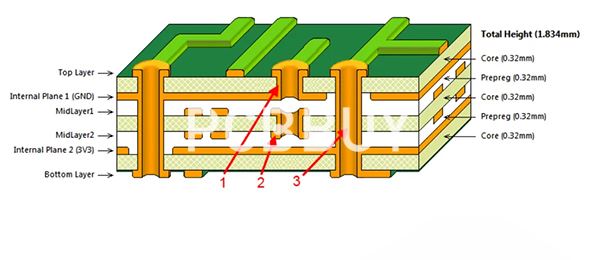
2. Choose Cost-Effective Materials and Via Structures
Material selection is another major cost factor. Standard FR-4 may be suitable for many industrial and control boards, while high-Tg or high-frequency laminates may be necessary for specific thermal or electrical requirements. Selecting premium material without a clear engineering need can increase cost, but substituting a specified material without validation can create reliability risks.
Via design also affects the manufacturing route. Conventional through-holes may be economical when they meet routing and electrical requirements. Blind and buried vias, microvias, and sequential lamination can support higher routing density, but may introduce additional process steps and inspection requirements.
|
Design factor |
Cost-conscious approach |
Engineering consideration |
|
Layer count |
Use only the layers needed for routing and performance |
Verify signal integrity, power integrity, and routing feasibility |
|
Laminate selection |
Prefer suitable, readily available materials |
Confirm Tg, dielectric properties, thermal needs, and customer requirements |
|
Via structure |
Use through-holes where practical |
Adopt HDI or blind/buried vias only when the design benefits justify the added complexity |
|
Copper weight |
Specify copper according to actual electrical and thermal demands |
Check current capacity, etching, and finished copper requirements |
|
Trace and space |
Avoid unnecessarily aggressive geometries |
Confirm manufacturability against the fabricator's process capability |
|
Panelization |
Arrange boards to improve usable panel area |
Consider board outline, spacing, tooling, and separation method |
3. Improve Panel Utilization and Manufacturing Yield
The price of a high-layer-count PCB is influenced not only by the cost of each board but also by how efficiently the design can be manufactured. Poor panel utilization, unnecessarily complex outlines, and tight tolerances that are not functionally required can increase cost or reduce yield.
When the product design allows, engineers can review board dimensions, orientation, spacing, and panelization with the fabricator. Standardized hole sizes and manufacturable clearances may also reduce process difficulty. For repeat orders, a stable, approved design helps prevent avoidable engineering changes and production interruptions.
PCBBUY provides DFM review and multilayer PCB manufacturing support. Its published capability information includes minimum mechanical hole sizes of 0.15 mm for standard drilling and customized smaller-hole evaluation for applicable designs; the final feasible hole size depends on the complete board construction. Published standard capabilities also identify a minimum line width of 35 μm (approximately 1.4 mil) in the supplied process specifications, but this should not be treated as a universal cost-optimal design rule.
For customers working with Lieban in automotive, industrial control, electrical power, power supplies, energy storage, new energy, and embodied robotics, reviewing manufacturability before design release can help balance performance, cost, and production consistency.
4. Match Inspection and Acceptance Criteria to the Application
Low fabrication cost is valuable only when the finished PCB meets the agreed requirements. High-layer-count boards need appropriate controls for layer registration, plated-hole quality, electrical continuity, insulation, and—where specified—controlled impedance.
Before production, customers and manufacturers should agree on the fabrication data, stackup, material specifications, copper thickness, finished-board dimensions, surface finish, and acceptance criteria. Inspection and testing should follow the purchase order, applicable IPC requirements, and customer-specific specifications.
PCBBUY's available quality processes include automated optical inspection (AOI), flying-probe electrical testing, and four-wire low-resistance testing where applicable. The required inspection scope should be confirmed for each project; additional tests should be specified when the application or customer standard requires them.
A clear acceptance plan helps prevent unexpected costs caused by rework, disputes, or qualification failure. For automotive and power-related products in particular, material changes and process deviations should be reviewed and approved through the appropriate engineering and quality procedures.
Conclusion
Low-cost high layer count PCB fabrication depends on engineering decisions made before manufacturing begins. Optimizing the layer stackup, choosing suitable materials, simplifying via structures where possible, improving panel utilization, and defining clear acceptance criteria can reduce avoidable costs without sacrificing performance.
PCBBUY supports multilayer PCB fabrication up to 26 layers, with material and process options evaluated against individual project requirements. Providing complete fabrication data early allows the engineering team to review manufacturability, identify potential cost drivers, and recommend practical options before production.
FAQ
1. What determines the cost of a high-layer-count PCB?
The main factors include layer count, laminate type, board dimensions, copper weight, finished thickness, drilling and via structures, minimum trace and space, surface finish, production quantity, and inspection requirements.
2. Can reducing the number of PCB layers lower fabrication cost?
Often, yes, because fewer layers may reduce material use and processing complexity. However, layer reduction must not compromise routing, impedance, power distribution, thermal performance, or reliability.
3. Are blind and buried vias always more expensive than through-holes?
They can increase cost because they may require additional drilling, lamination, or filling processes. They are justified when routing density, component escape, or electrical requirements cannot be met effectively with conventional through-holes.
4. What high-layer-count PCB capability does PCBBUY offer?
PCBBUY's published standard capability lists PCB fabrication from 1 to 26 layers, with material options including FR-4, high-Tg FR-4, halogen-free materials, and selected Rogers high-frequency laminates. The specific construction should be confirmed through engineering review.
5. How can I obtain a cost-effective quotation for a high-layer-count PCB?
Provide the Gerber files, stackup, board dimensions, material and Tg requirements, copper weights, finished thickness, via details, surface finish, quantity, impedance requirements, and applicable acceptance criteria. Complete information helps the manufacturer evaluate process feasibility and identify realistic cost-optimization opportunities.
Industry Category