Main Types of Vias in PCB: A Comprehensive Guide
By: 05/29/2025 15:23
Introduction
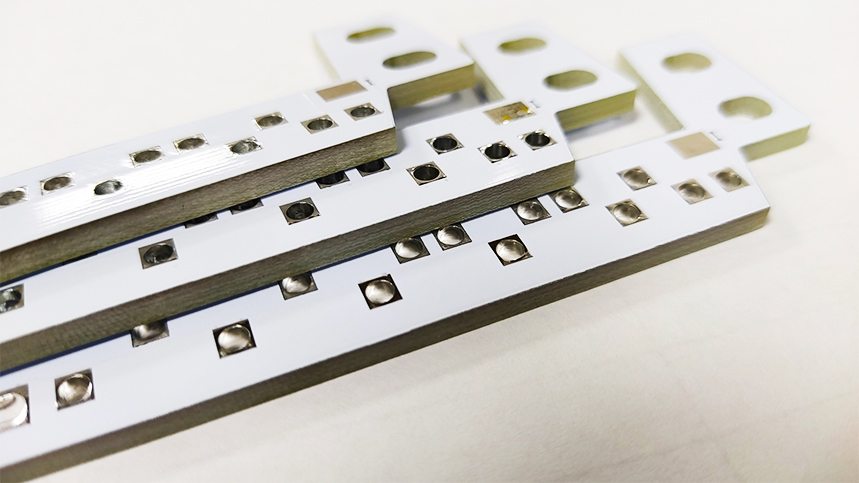
Printed Circuit Boards (PCBs) rely on vias to enable electrical connectivity between different layers, signal routing, and component attachment. As electronic devices shrink in size while increasing in complexity, the role of vias has become critical in determining performance, reliability, and manufacturability. This article provides an in-depth analysis of the primary via types, their fabrication principles, technical specifications, and applications, supported by data and industry standards.
1. Through-Hole Vias (Plated Through Holes, PTH)
Principle and Fabrication
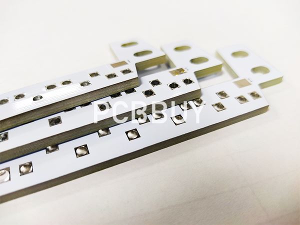
Through-hole vias are the most traditional type, penetrating all layers of a multilayer PCB. Their fabrication involves:
-
Mechanical Drilling: A CNC drill creates holes (typical diameter: 0.1–5 mm).
-
Electroless Plating: Deposition of a copper seed layer for adhesion.
-
Electroplating: Buildup of copper to fill the hole and connect internal layers.
Key Characteristics
-
Size: Diameters >150 μm (common in standard PCBs).
-
Resistance: ~0.1–1 ohm per via (dependent on length and plating thickness).
-
Capacitance: ~0.5–2 pF (affects high-speed signals).
-
Cost: Lowest among via types due to simplicity.
Applications
-
General-purpose PCBs (e.g., consumer electronics).
-
Low-density designs where space constraints are minimal.
Limitations
-
Large footprint restricts miniaturization.
-
Parasitic capacitance and crosstalk in high-frequency applications (>10 GHz).
2. Microvias
Principle and Fabrication
Microvias are smaller than through-hole vias, designed for high-density interconnects (HDI). Two main types exist:
-
Laser-Drilled Vias: Created using UV lasers (diameter: 10–100 μm).
-
Photo-Defined Vias: Formed via photolithography (subtractive etching of dielectric layers).
Key Characteristics
-
Size: <100 μm diameter, enabling tighter trace spacing.
-
Resistance: ~0.05–0.5 ohm (lower than through-hole vias).
-
Capacitance: ~0.1–0.5 pF (reduced signal delay).
-
Cost: Higher due to precision manufacturing.
Applications
-
HDI PCBs (e.g., smartphones, tablets).
-
Layer transitions in fine-line boards.
Technical Challenges
-
Aspect Ratio: Hole depth-to-diameter ratios >1:1 require precise electroplating.
-
Reliability: Microcracks or voids in copper filling can lead to failure.
3. Blind and Buried Vias
Principle and Fabrication
-
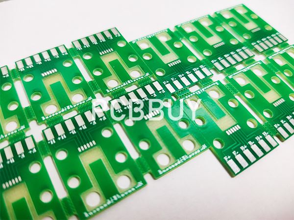
Blind Vias: Connect an external layer to an inner layer without穿透整个板.
-
Buried Vias: Connect two inner layers, hidden within the stack.
Both require advanced HDI processes, such as:
-
Sequenced Lamination: Partial dielectric deposition.
-
Laser Ablation: Selective removal of dielectric materials.
Key Characteristics
-
Blind Via Diameter: 50–200 μm.
-
Buried Via Diameter: Similar to microvias but with stricter alignment tolerances.
-
Layer Transition: Enable >90% space savings compared to through-hole vias.
Applications
-
High-layer-count PCBs (e.g., server motherboards).
-
Miniaturized devices requiring complex signal routing.
Data Support
|
Via Type |
Diameter (μm) |
Aspect Ratio |
Typical Resistance (ohm) |
Application Example |
|
Blind Via |
75–150 |
1:1–1:2 |
0.1–0.3 |
Smartphone PCB |
|
Buried Via |
50–120 |
1:1.5–1:3 |
0.05–0.2 |
Advanced server board |
4. Specialty Vias
4.1 Back-Drilled Vias
-
Purpose: Eliminate unused through-hole segments to reduce parasitic capacitance.
-
Process: Mechanical drilling followed by laser drilling from the backside.
-
Benefit: Improves signal integrity in high-speed designs (e.g., 5G antennas).
4.2 Mixed-Dielectric Vias
-
Structure: Composite dielectric materials (e.g., polyimide + ceramic) for controlled dielectric constant (Dk).
-
Application: High-frequency PCBs (e.g., radar systems).
4.3 Plated Palladium/Silver Vias
-
Function: Enhance conductivity and corrosion resistance for harsh environments.
-
Data: Palladium-plated vias exhibit ~30% lower resistivity than standard copper vias.
Comparison and Selection Criteria
Table 1: Key Metrics for Via Types
|
Parameter |
Through-Hole Vias |
Microvias |
Blind/Buried Vias |
Specialty Vias |
|
Diameter (μm) |
150–5,000 |
10–100 |
50–200 |
Varies (50–500) |
|
Resistance (ohm) |
0.1–1 |
0.05–0.5 |
0.05–0.3 |
0.01–0.5 |
|
Capacitance (pF) |
0.5–2 |
0.1–0.5 |
0.1–0.3 |
<0.1 (back-drilled) |
|
Cost (USD/via) |
0.01–0.05 |
0.1–0.5 |
0.5–1.0 |
1.0–5.0 |
|
Best For |
General PCBs |
HDI, fine pitch |
High-layer-count |
High-freq, durability |
Selection Guidelines
-
Density Needs: Through-hole vias for low density, microvias for HDI.
-
Signal Frequency: Back-drilled or mixed-dielectric vias for high-speed signals.
-
Environment: Palladium/silver vias for automotive or industrial applications.
-
Budget: Through-hole vias for cost-sensitive projects.
Advanced Considerations
Signal Integrity
-
Impedance Control: Via stubs (unused segments) cause impedance mismatches. Back-drilling reduces stub length, maintaining characteristic impedance (Z0) within ±10%.
-
Crosstalk Mitigation: Ground vias shield adjacent signal vias, reducing coupling by ~20 dB.
Thermal Management
-
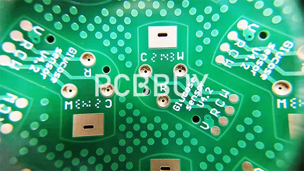
High-density vias concentrate heat; thermal vias (multiple vias grouped) dissipate heat from components (e.g., CPUs).
-
Data: A cluster of six thermal vias reduces local temperature by ~15°C.
Reliability Testing
-
Thermal Cycling: IPC-TM-650 standard requires vias to withstand -40°C to +125°C for >500 cycles.
-
Mechanical Strength: Pull-out force >10 N for through-hole vias, >5 N for microvias.
Future Trends
-
Nano-Vias: Research into sub-10 μm vias using electron beam lithography.
-
Additive Manufacturing: 3D printing of vias with conductive inks (prototypes show ~50% cost reduction).
-
Biodegradable Materials: Eco-friendly vias using plant-based dielectrics (currently in development).
Conclusion
The selection of via types is a critical trade-off between performance, cost, and manufacturability. As technology advances, innovations like laser micromachining and hybrid dielectrics are pushing the boundaries of via miniaturization and functionality. For designers, understanding these nuances ensures optimal PCB performance in diverse applications.
References
-
IPC Standards: IPC-2221/2222 (PCB Design Guidelines), IPC-TM-650 (Test Methods).
-
Smith, J. et al. (2024): High-Density Interconnect Technologies: Advances in Via Reliability, IEEE Transactions on Components and Packaging Technologies.
-
Market Data: Prismark Report (2024): Global PCB Industry Trends.
-
Material Science: Hayakawa, Y. (2023): Dielectric Materials for High-Frequency Vias, Journal of Electronic Materials.
-
Laser Processing: Schmidt, R. et al. (2022): Precision Laser Drilling for Sub-50 μm Vias, SPIE Proceedings.
Industry Category


