Minimum Trace Spacing in PCB Design Guide
By:PCBBUY 11/28/2025 17:19
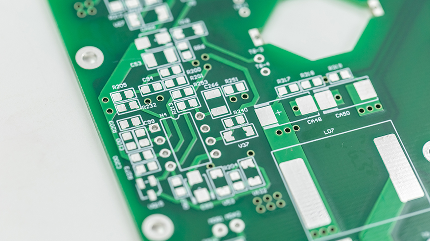
Minimum trace spacing refers to the smallest manufacturable clearance between two adjacent copper features. This parameter determines electrical safety, signal integrity performance, and manufacturability limits in high-density PCB designs.
As a PCB manufacturer serving global clients, PCBBUY often receives questions about ideal spacing, manufacturable limits, and how spacing affects cost. This article gives you a clear, beginner-friendly explanation while showing you the spacing capabilities we offer.
What Is Minimum Trace Spacing?
Minimum trace spacing refers to the narrowest allowed distance between two copper traces on a PCB. This spacing ensures that:
-
signals do not interfere with each other
-
high-voltage circuits stay safe
-
copper does not short during soldering or assembly
-
the PCB can be produced accurately by the factory
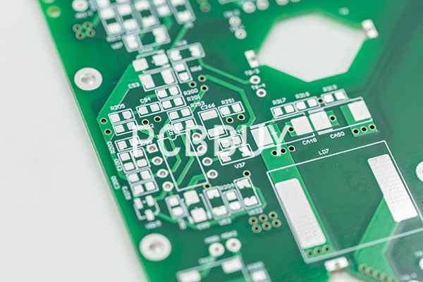
In simple terms: the smaller the trace spacing, the more difficult the board is to manufacture — especially for HDI or ultra-dense designs.
Industry Standards for Trace Spacing
Most PCB designers follow IPC standards, which give clear spacing recommendations. For example:
-
General electronics (IPC Class 2): 4–5 mil
-
High-end or mission-critical devices (IPC Class 3): 3–4 mil
-
High-voltage applications: spacing increases based on voltage requirements
-
High-speed circuits: spacing is often larger to reduce crosstalk
These values are general guidelines — actual manufacturability depends on the PCB factory’s equipment and process control.
What Factors Affect Minimum Trace Spacing?
The ideal spacing depends on a few real-world conditions:
1. Voltage
Higher voltage requires more clearance to prevent arc or breakdown.
2. Signal Speed
High-frequency or differential signals need more spacing to prevent interference.
3. Copper Thickness
Thicker copper requires more spacing due to etching limits.
4. PCB Material
High-frequency materials like Rogers allow cleaner etching compared to standard FR4.
5. Fabrication Capability
This is where PCB factories differ the most.
PCBBUY Minimum Trace Spacing Capabilities
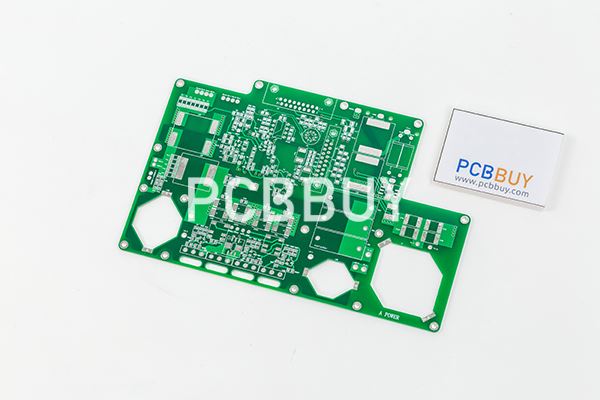
PCBBUY supports a wide range of line/space capabilities to fit different markets and cost levels:
|
PCB Type |
Minimum Line/Space |
Notes |
|
Standard FR4 |
4/4 mil |
Stable for mass production |
|
Advanced FR4 |
3.5/3.5 mil |
Tight tolerance |
|
HDI PCB |
3/3 mil |
LDI exposure technology |
|
High-density / on request |
2.5/2.5 mil |
For premium devices |
Why PCBBUY can achieve this:
-
Automatic LDI exposure
-
Controlled etching and cleaning lines
-
AOI inspection for micro-lines
-
Strict DFM checks before production
This combination ensures reliable fine-pitch boards with consistent quality.
Design Tips for Better Trace Spacing
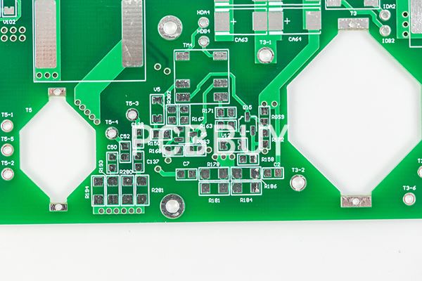
If you're designing boards for reliable production, consider these tips:
-
Follow IPC spacing rules
-
Give more spacing to high-speed or sensitive signals
-
Keep differential pair spacing uniform
-
Use DRC rules inside Altium, KiCad, Eagle, or Cadence
-
Ask your manufacturer for DFM advice before finalizing the design
PCBBUY’s engineering team offers free DFM checks, helping designers reduce risk and avoid redesigns.
Why Choose PCBBUY?
✔ Stable fine-line capability
✔ Experienced with HDI and high-density consumer electronics
✔ Professional engineering review before production
✔ Fast prototyping + high-volume manufacturing
✔ Competitive pricing for global customers
No matter what industry you work in, PCBBUY can provide reliable minimum spacing solutions.
Conclusion
Minimum trace spacing is more than a rule — it's essential for signal integrity, safety, and manufacturability. With PCBBUY’s advanced production capabilities and strong engineering support, designers can confidently build boards with both standard and fine-pitch spacing.
FAQ
Q1: What is the recommended minimum trace spacing in PCB design?
Most PCB factories recommend 4 mil for standard boards and 3 mil for HDI boards.
Q2: Can PCBBUY manufacture PCBs with 3 mil spacing?
Yes. PCBBUY supports 3/3 mil for HDI and fine-line applications.
Q3: Does smaller spacing increase PCB cost?
Yes — finer spacing requires LDI exposure and tighter process control.
Q4: Do high-voltage circuits need larger spacing?
Correct. Higher voltage requires more clearance to prevent electrical breakdown.
Q5: What software can check spacing automatically?
Altium, KiCad, Eagle, Cadence, and almost all ECAD tools support DRC spacing rules.
Industry Category


