Multi Layer Pcb
By: 03/11/2021 14:13

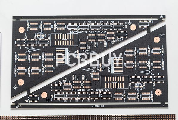
The double-sided board is the middle layer of media, and both sides are trace layers. A multi-layer board is a multi-layer wiring layer. Between each two layers is a dielectric layer. The dielectric layer can be made very thin. The multilayer circuit board has at least three conductive layers, two of which are on the outer surface, and the remaining layer is synthesized in the insulating board. The electrical connection between them is usually achieved through plated through holes in the cross section of the circuit board.
A multilayer printed circuit board is a circuit board composed of two or more conductive layers (copper layers) superimposed on each other. The copper layer is bonded together by a resin layer (prepreg). Multi-substrate is the most complicated type of printed circuit board product. Due to the complexity of the manufacturing process, lower production volume and difficulty in redoing, their prices are relatively high.
Due to the increase in the packaging density of integrated circuits, it leads to a high concentration of interconnect lines, which makes the use of multiple substrates necessary. In the layout of the printed circuit, unforeseen design problems have appeared, such as noise, stray capacitance, and crosstalk. Therefore, the design of printed circuit boards must focus on minimizing the length of signal lines and avoiding parallel routes. Obviously, in a single-sided PCB or even a double-sided board, these requirements cannot be answered satisfactorily due to the limited number of crossovers that can be achieved. In the case of a large number of interconnections and cross-over requirements, to achieve a satisfactory performance of the PCB circuit board, the board layer must be expanded to more than two layers, so a multilayer circuit board has appearanced. Therefore, the original intention of manufacturing multi-layer circuit boards is to provide more freedom for selecting suitable wiring paths for complex and/or noise-sensitive electronic circuits.
The multilayer circuit board has at least three conductive layers, two of which are on the outer surface, and the remaining layer is synthesized in the insulating board. The electrical connection between them is usually achieved through plated through holes on the cross section of the circuit board. Unless otherwise stated, multi-layer printed circuit boards, same as double-sided boards, are generally plated through-hole boards.
The manufacturing method of the multi-layer board is generally made by the inner layer pattern first, and then the single-sided or double-sided substrate is made by the printing etching method, and it is included in the designated layer, and then heated, pressed and bonded, as for the subsequent The hole is the same as the double-sided plated through-hole method. It was invented in 1961.
Simple differentiation of multilayer circuit boards
The circuit board determines the process difficulty and processing price according to the number of wiring surfaces. The ordinary circuit board is divided into single-sided circuit and double-sided circuit. It is commonly known as single-sided board and double-sided board. In addition to the surface circuit, multiple layers of circuits can be superimposed inside. During the production process, after each layer of circuit is made, it is positioned and pressed by optical equipment, so that the multilayer circuit is superimposed on a circuit board. Commonly known as multilayer circuit boards. Any circuit board greater than or equal to 2 layers can be called a multilayer circuit board. Multilayer circuit boards can be divided into multilayer rigid circuit boards, multilayer flex-rigid printed circuit boards .

The birth of multilayer circuit boards
Multi-substrates are manufactured by stacking two or more circuits on top of each other, with reliable pre-defined interconnections between them. Since drilling and electroplating have been completed before all layers are rolled together, this technique violates the traditional manufacturing process from the beginning. The innermost two layers are composed of traditional double boards, while the outer layers are different. They are composed of independent single boards. Before rolling, the inner substrate will be drilled, plated through, pattern transferred, developed and etched. The outer layer to be drilled is the signal layer, which is plated in such a way that a balanced copper ring is formed on the inner edge of the through hole. The layers are then rolled together to form a multi-substrate, which can be interconnected (between components) using wave soldering.
Rolling may be done in a hydraulic press or in an overpressure tank (autoclave). In a hydraulic press, the prepared material (for pressure stacking) is placed under cold or preheated pressure (high glass transition temperature material is placed at a temperature of 170-180°C). The glass transition temperature is the temperature at which the amorphous region of an amorphous polymer (resin) or part of a crystalline polymer changes from a hard, rather brittle state to a viscous, rubbery state.
Industry Category


