Multilayer PCB Stackup
By:PCBBUY 08/16/2021 17:17

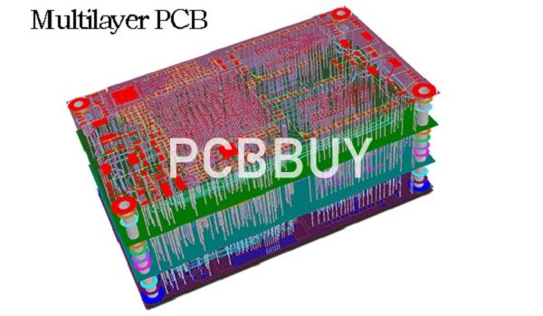
Stack-up describes the construction of a multilayer board in sequential order. It provides vital information like material thickness and copper weights required to fabricate a PCB. Stack-ups are also referred to as build-ups. The stack-up also gives the details of trace width for different controlled impedance traces such as 50ohms, 100ohms differential. An example of a 6-layer stack-up is shown in the above image.
In this passage, we will focus on the multilayer PCB stackup. If you are curious about it please check and read the content we provide to learn more professional information.
If you want to order PCB product, please check and custom your order online.
What are the different layers in a multilayer PCB?
A stack-up primarily consists of metal foil, prepreg, and copper-clad laminate (core).
Metal foil: Copper is the most commonly used metal foil in PCB construction.
Prepreg: It is an interwoven glass cloth impregnated in epoxy resin. The resin is left semi-cured.
Copper-clad laminate: Single or multiple plies of prepreg bonded together along with the top and bottom copper foil makes a copper-clad laminate. This is also known as the core.
What are the power and ground layers in multilayer PCB stackup?
The power plane is a copper layer connected to the power supply. It is often designated as VCC in PCB design. The main function of the power plane is to provide a steady voltage supply to the PCB. In multi-layered boards, if a component needs to draw power then it is simply connected to the via that makes contact with the power plane. Similarly, the ground plane is a plane of flat copper connected to the common ground point in the PCB.
Advantages of using power/ground planes
1. The power and ground pins of the components can easily be connected to the power and ground planes.
2. It provides a clear current return path, especially for high-speed signals. This in turn reduces the EMI (electromagnetic interference).
3. The power planes have a larger current carrying capacity than the traces. This also reduces the operating temperature of the PCB.
What is PCB lamination?
The lamination is the process of placing the stack-up under extreme temperature and pressure to bond prepreg and copper foil to the base PCB inner layers. The temperature and pressure values are mentioned in the datasheets of the chosen PCB materials.
What is the standard board thickness?
The thickness of a PCB mainly depends on factors such as copper thickness, materials used, number of layers, and the operating environment. The standard thickness of a conventional board is around 62 mils (1.57mm). Today, PCBs have become more complex as the copper layer weight and the layer count have increased for various applications. Due to this, the PCBs tend to become thicker. Manufacturers, based on the customer’s request, are now fabricating PCBs with two new standard thicknesses, 93 mils (2.36mm) and 125 mils (3.17mm) (150% and 200% of old standard thickness).
Why we need multilayer PCB?
In this modern era, electronic devices are becoming more complex and consist of a higher number of components and circuits. It becomes a tedious task to accommodate the complex circuits in a single-layered PCB. This problem can be solved by adding layers to the stack-up.
Let us have a look at few advantages of multilayer boards:
1. They are capable of accommodating complex circuits that are required for modern electronic devices.
2. Having more layers means the board is thicker and, therefore, more durable than single-sided PCBs.
3. Multi-layer boards require more planning and intensive production processes, so they are of a higher quality than other types of boards.
4. Using multiple PCB components would require multiple connection points. Multi-layer boards, on the other hand, are designed to work with a single connection point, simplifying the design of the electronic device and further reducing the weight.
How to build multilayer PCB stackup?
Step 1: Inner layer core selection
The stack-up designates the materials to be used for the manufacture of a multilayer circuit board. The build-up provides the following information:
·The copper thickness and weight
·Type of epoxy glass to be used
·Panel size
Step 2: Cleaning
The inner layers are cleaned chemically/mechanically or both to remove contaminants from the copper surface.
Step 3: Inner layer imaging
The imaging material is placed on the copper surface. It covers the desired copper circuitry and exposes the unwanted copper.
Step 4: Etch stripping
The inner layers are chemically etched to get rid of the unwanted copper. The photoresist is then stripped off to reveal the copper circuitry.
Step 5: Automated Optical Inspection
Automated optical inspection is carried out to find the flaws(shorts/opens in inner layers) that can’t be detected by the human eye.
Step 6: Oxide treatment
The exposed copper circuitry on the inner layer must be treated before lamination to improve adhesion. Improved adhesion also increases the structural strength and overall board reliability.
Step 7: Layup
Steps 1 to 6 are repeated for all the inner layers. For example, these steps will be carried for layers 2, 3, and 4, 5.
Step 8: Lamination
In this step, the stacks are pressed and heated in a vacuum chamber. The Lamination process begins by applying vacuum to remove all the entrapped air and gases. Later, heat and pressure are applied to the stack so the resin in the prepreg undergoes a molecular bonding.
Step 9: Drilling
After the lamination process, the laminated board is loaded on a panel of exit material on the drill bed. The holes are drilled on the PCB to make vias and through holes. The exit material lessens the burr formation. Burr is the protruding part of copper formed when the drill spindle penetrates through the board.
Industry Category


