PCB Annular Ring Size
By:PCBBUY 08/25/2021 09:07

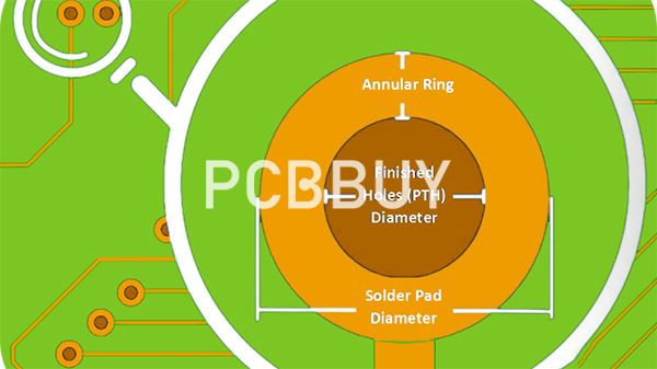
An annular ring is the area of copper pad around a drilled and finished hole. The finished hole we are talking about here is nothing but a copper-plated via. All around this via there should be enough copper to form a solid connection between the copper traces and the via in a multi-layer PCB. Therefore, the main purpose of an annular ring is to establish a good connection between a via and the copper trace.
Are you going to learn more about PCB annular ring size?Check and read this passage for more professional knowledge. Let’s go!

Why size is important to PCB annular ring?
The width of the ring should be sufficiently thick to allow reliable electrical connection with via. The minimum length of the ring should be greater than or equal to the specified width for the design. A dimension that is less than the value specified in the design can interfere with the attachment of the component. It can also lead to pad breakout (zero annular ring), a condition associated with the region where the circuit enters the pad. This can reduce the current-carrying capacity of the circuit.
· Common annular ring issues
· Undesired annular ring
· Tangency
· Breakout
What are the common issues of PCB annular ring?
Common issues with the annular rings
A perfect annular ring will be created by drilling right into the center of the via pad. However, the annular ring may not be in the center because the drilling accuracy depends on the drilling machine used by the PCB manufacturer. There are several drill issues with the annular ring:
Good via
When the via is in the center of the pad or the given limit area, we call the via is a good via, which will result in a nice donut-shaped annular ring and good electrical connectivity.
Tangency:
When the driller is not aligned with the mark, the finished hole will be off-center and near the side of the pad. An annular ring tangency will appear when a part of the hole contacts the edge of the pad.
Breakout:
If the hole deviates a lot, a breakout occurs when a portion of the hole exceeds the padded area. This is a kind of undesired annular ring, which may cause short circuits and failure connectivity.

How to calculate PCB annular ring?
While it is true that PCB makers are responsible for manufacturing accurate designs, designers also play a huge role. Designers matter when it comes to coming up with the right size designs. Without the correct annular ring sizes, then the overall functionality of the board is at risk. Ensuring the correct annular ring sizes will save you from heartaches later.
Determine the type according to needs
PCBs, find a lot of use in many applications based on their high boiling points and electrical insulating properties. They find heavy use in heat transfer, electrical, and hydraulic equipment. Lately, you can find the use of PCBs in home appliances, military, and medical equipment. When calculating the PCB annular ring, you need to factor in where it will find its use. The type of the annular ring depends on the needs of your PCB quote.
If your printed circuit board requires special requirements, then it may require high-quality PCB annular rings. The Institute of Printed Circuit boards lists three essential classes of PCBs. There are Class 1, 2, and 3 PCB products; level 3 ones find heavy applicability instead of Class 1 and Class 2 products. For this reason, Class 3 annular ring requirements are slightly different. Their pad sizes need to be more significant enough to accommodate via’s diameter.
Design criteria of PCB annular ring
Without the right design criteria for PCB annular rings, you may end up with a board with poor functionality. It would help if you got everything right so that your equipment functions as desired.
Calculation formula
The calculation formula of PCB annular rings isn’t as complicated as you may think. Unfortunately, though, many people aren’t aware of arriving at such calculations. For reasons of creating via, it means that the drilled hole requires a copper surrounding. The ring of copper is the via size or the outer diameter. According to IPC-2221A standards, the calculation of the minimum PCB annular ring size is as follows:
Minimum Annular Ring = (Min Ringer Border) * 2 + (Tolerance) + (Hole Size)
The annular PCB ring is (diameter of the pad – the hole) /2. Assume that you have a pad diameter of 20 mils and a hole diameter of 10 mils. For this reason, the annular ring width will be 20 – 10 = 5 mils.
Minimum annular ring
You need to pay attention to the minimum ring width. It is important to note that there’s a minimum annular ring on the inner and outer layers of a PCB. Most designers agree on a minimum annular ring of 0.1mm on the inner layers of a PCB. Also, most PCB designers agree on 0.05mm as the minimum annular ring on the outer layer.
If you want to achieve the best and most desirable minimum annular rings, then you’ll need to consider a few things. But the most important thing is to ensure that you work with a designer who values Design for Manufacturability (DFM). With DFM, you’ll acquire PCBs with the minimum size of the annular ring.
Industry Category


