PCB Buried Via Technology Advanced Manufacturing Capabilities
By:PCBBUY 08/26/2025 16:11
Introduction to PCB Buried Via
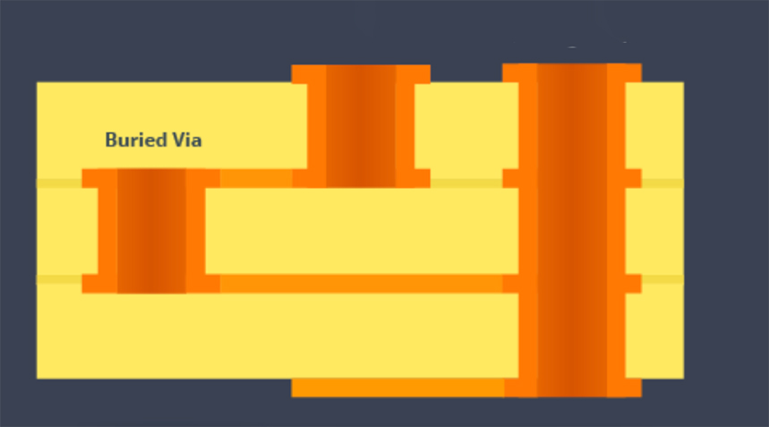
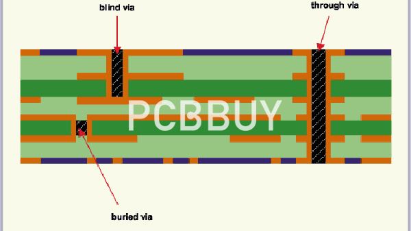
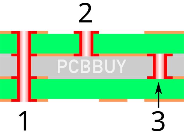
In modern electronics, where devices are becoming smaller and more powerful, the demand for advanced printed circuit board (PCB) technologies continues to grow. Among these technologies, PCB buried via plays a critical role in enabling high-density interconnection (HDI) designs. Unlike through-hole vias or blind vias, buried vias connect only the inner layers of a PCB without appearing on the external layers. This allows designers to maximize routing density and save valuable surface space for components.
At PCBBUY, we specialize in providing cutting-edge PCB buried via manufacturing solutions, ensuring high precision, reliability, and scalability for a wide range of applications.
Why PCB Buried Via is Essential in Modern Electronics
The use of PCB buried vias brings significant advantages to electronic product design and manufacturing:
-
Space Optimization: Buried vias free up the outer layers for critical signal routing and component placement.
-
Improved Signal Integrity: By isolating connections within the PCB stack-up, buried vias minimize parasitic effects and signal interference.
-
Support for Complex Designs: Essential for HDI PCBs used in 5G communications, automotive electronics, servers, consumer devices, and medical instruments.
-
High Reliability: Properly manufactured buried vias enhance long-term durability under mechanical and thermal stress.

PCB Buried Via Manufacturing Process at PCBBUY
1. Design Stage Considerations
Before production, our engineering team works closely with customers to evaluate the stack-up and define via placement. For 1st order buried via, structures such as 1+N+1 or 1+1+N+1+1 are typically used, where the buried vias are ≤0.3 mm. For 2nd order buried via, examples include 2+N+2 or 1+2+N+2+1, ensuring multi-layer buried via solutions that meet advanced interconnect requirements.
2. Drilling and Via Formation
-
Mechanical Drilling: Preferred for standard buried via structures, ensuring stable accuracy.
-
Laser Drilling: Used for micro-vias or extremely small diameters.
-
Hole diameters are carefully controlled, and aspect ratios are optimized to maintain plating quality.
3. Copper Plating and Filling
Based on the customer’s laminated structure, PCBBUY uses mechanical via plating as the first choice. If structural limitations arise, electroplating via filling process is applied to guarantee conductivity and via reliability. The plating ensures smooth copper walls, uniform thickness, and strong metallurgical bonding.
4. Lamination Process
The multi-stage lamination process bonds the PCB layers together. Buried vias are embedded between layers during lamination, ensuring high structural strength and electrical stability. PCBBUY utilizes advanced sequential lamination technology to handle complex multi-order buried via designs.
5. Inspection and Testing
Every buried via undergoes rigorous inspection using:
-
X-Ray Inspection: To confirm internal via alignment and plating quality.
-
AOI (Automated Optical Inspection): For layer-to-layer connection accuracy.
-
Reliability Testing: Thermal cycling, cross-section analysis, and electrical performance validation.
PCBBUY’s Technical Capabilities in PCB Buried Via Manufacturing
As a professional PCB manufacturer, PCBBUY offers advanced buried via technology with the following highlights:
-
Via Diameter: Buried vias as small as 0.1 mm, supporting high-density interconnects.
-
Aspect Ratio: Up to 10:1 standard, with customization available up to 20:1 depending on customer requirements.
-
Multi-Order Buried Vias: Support for both 1st order and 2nd order buried via structures.
-
High-Layer Count PCBs: Reliable buried via manufacturing for up to 40+ layers.
-
Certified Manufacturing: ISO, UL, and RoHS compliance ensures international standards for quality and safety.
Advantages of Choosing PCBBUY for PCB Buried Via
-
Precision and Reliability: Advanced drilling and plating technology ensures consistent buried via performance.
-
Flexible Customization: From prototypes to mass production, PCBBUY offers tailored solutions.
-
Rapid Turnaround: Efficient production lines for both small batches and high-volume manufacturing.
-
Global Customer Base: Trusted by clients in telecommunications, automotive, aerospace, and consumer electronics.
Challenges in PCB Buried Via Manufacturing and PCBBUY Solutions
Challenges
-
Alignment accuracy in multilayer lamination.
-
Risk of voids or uneven copper plating inside vias.
-
Structural deformation during high-temperature lamination.
PCBBUY Solutions
-
High-precision drilling and laser alignment systems.
-
Advanced electroplating control for uniform via filling.
-
Multi-stage lamination under strict thermal management.
-
100% quality inspection using AOI and X-ray testing.
Future Trends of PCB Buried Via Technology
The demand for smaller, faster, and more reliable devices is pushing PCB buried via technology forward. Future trends include:
-
Smaller buried via diameters (<0.1 mm).
-
Higher aspect ratios for ultra-thin PCBs.
-
Integration with advanced materials for 5G and AI applications.
PCBBUY continues to upgrade production capabilities to stay ahead of these trends and deliver cutting-edge solutions for global customers.
Conclusion
PCB buried via technology is essential for achieving high-density, high-performance PCB designs. With its advanced equipment, strict quality control, and extensive experience, PCBBUY provides reliable buried via solutions that support complex designs in telecommunications, automotive, aerospace, and beyond.
If you are looking for a trusted partner for PCB buried via manufacturing, PCBBUY is your reliable choice. Contact us today to explore customized solutions for your next-generation electronics.
FAQ: PCB Buried Via
1. What is the difference between buried via and blind via?
Buried vias connect only inner layers and are invisible from outside, while blind vias connect outer to inner layers.
2. What is the typical aspect ratio for PCB buried vias?
PCBBUY supports up to 10:1 as standard, with custom options up to 20:1.
3. How does PCBBUY ensure buried via reliability?
Through advanced plating, lamination, and rigorous X-ray inspection.
4. What industries benefit from buried via PCBs?
5G telecom, automotive electronics, aerospace, servers, and medical equipment.
5. Can PCBBUY provide prototypes with buried vias?
Yes, PCBBUY supports both quick-turn prototypes and mass production.
Industry Category


