PCB Component Orientation
By:PCBBUY 08/24/2021 09:27

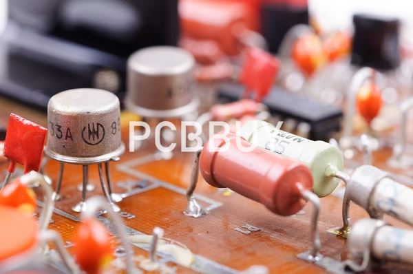
At one time, the slower circuitry of older circuit boards allowed PCB designers a lot more latitude in how they placed their components. If we have components that aren’t aligned with the correct orientation, there could be a lot of damage when it comes to getting the board assembled. Here is some more information on those guidelines and how you can ensure you have the correct component orientation on PCB designs.
In this passage, we will provide the information of PCB component orientation. If you are searching the knowledge of PCB, check and read the content below to learn more.
What are the main considerations for PCB component orientation?
There are three primary goals that your PCB contract manufacturer will focus on when they review your design for manufacturability:
· Standardization: By making sure that your PCB design will fit into a standard assembly process, your CM can reduce the labor and time involved, which lowers your cost.
· Assembly problems: By eliminating known potential assembly issues, your CM will improve production yields and once again pass on cost savings to you.
· Quality: By identifying and replacing parts or materials that could be potentially defective from the assembly process, your CM can once again improve yields.
During the DFM review, one of the details of your PCB that will be looked at to achieve these goals is component orientation. The rotation of parts on a PCB can have a great effect on its manufacturability, starting with the soldering process.
What are the guidelines of PCB component placement?
Before going into the specifics of component placement and orientation, there are several general guidelines to keep in mind:

· Orient similar components in the same direction.
· Avoid placing components on the solder side of a board.
· Try to place all your SMT components on the same side of the board, and all the through-hole components (if mixed) on the top side of the board.
· When you have mixed technology components (SMT and PTH), manufacturers might require an extra process to epoxy the bottom components.
· You should terminate all lands with only one trace.
· When you specify a chip under a device, this can make inspections, rework, and test more difficult.
· All components used on the wave solder sides of an assembly should first be approved by your manufacturer for immersion in a solder bath.
How component orientations affect PCB?
At one time, a circuit board could be laid out with its parts arranged aesthetically and it would perform just as well. However, that is no longer the case—today, PCB quote components must be placed in specific partitions according to their function for optimum performance. They also have to be oriented correctly to satisfy the needs of the signal or power circuitry they are servicing.
High-Speed Signals
There is more to a high-speed circuit than just a single point-to-point connection. High-speed circuitry often consists of multiple nets that together make up one complete signal path. For instance, a signal path may start at a source and then go through a resistor before terminating at its load. Therefore, the signal path consists of two nets with a resistor in the middle, and for the best signal integrity, both nets need to be treated together as one. To accomplish this, the resistor must be oriented to provide the most optimum connection between the signal path’s two nets.

High-speed routing also consists of memory and data buses that contain many nets. Not only do these nets need room for their trace routing, but for escape vias as well. This requires that all components connected to these nets be orientated in the most optimum direction for the shortest possible trace routing. In the same way, components that are part of impedance controlled nets must be oriented for the shortest and most direct connections, especially those that need to be routed with differential pairs.
Power Supplies
Power supply components must also be oriented for the most optimum connection configuration during placement. To reduce the inductance and resistance as well as the noise that can be created in high current power supply traces, the routing must be as short and as direct as possible. This will require a very tight placement of the power supply parts and possibly some unusual component orientations. Additionally, power supply components should also all be placed on the same side of the board to help with the short and direct routing.
Satisfying all of these signal and power integrity needs will require some creative placement of the PCB components. Some of these parts may end up having to be orientated at odd angles instead of the usual 90-degree increments to achieve the best signal and power routing. The key is to check first with your manufacturer to see what they can and can’t build before starting your board placement.
What are the rules of PCB component placement?
Place the main components as per signal flow.
Refer to the schematic circuit diagram while placing the components. Identify the main components of the circuit such as microprocessors, Ethernet chips, memories, etc.
Place these as per the floorplan and with the shortest traces between these main chips as per the datasheet guidelines and which makes the signal flow smooth and unidirectional as far as possible.

Place the associated components near the main components
Next, place the components associated with the main components such as crystal oscillators, decoupling capacitors, termination resistors.
Industry Category


