PCB Copper Clad Laminate and Manufacturing Capability
By:PCBBUY 12/31/2025 16:56

Introduction
In PCB manufacturing, material selection plays a decisive role in electrical performance, mechanical stability, and long-term reliability. Among all base materials, PCB copper clad laminate serves as the foundation on which all circuit structures are built.
Understanding copper clad laminate properties and processing requirements helps designers and buyers evaluate a PCB manufacturer’s true technical capability.
What Is PCB Copper Clad Laminate?
PCB copper clad laminate (CCL) is a composite material consisting of a dielectric substrate bonded with copper foil on one or both sides. It is the starting material used to fabricate printed circuit boards through imaging, etching, drilling, and lamination processes.
Copper clad laminate determines the physical and electrical baseline of the PCB before any circuitry is formed.
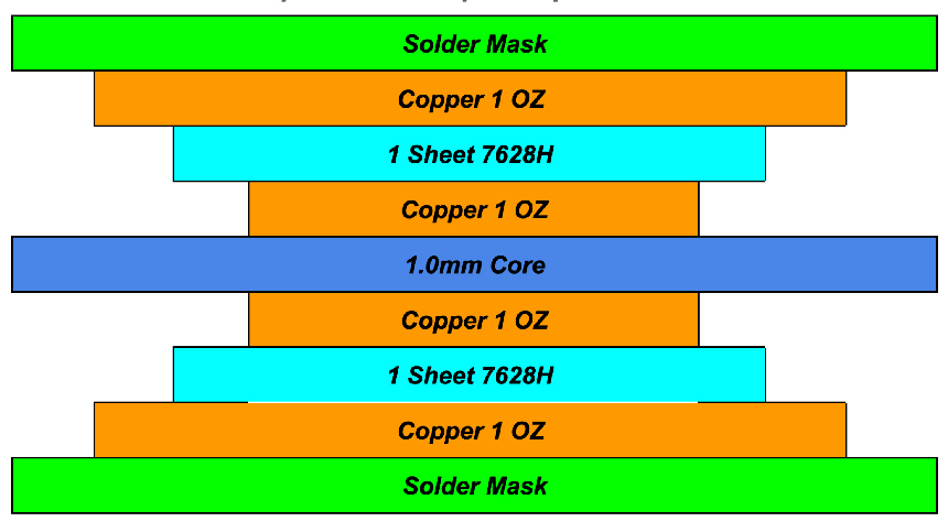
Basic Structure of Copper Clad Laminate
A typical PCB copper clad laminate includes:
-
Copper foil layer (electrical conductor)
-
Dielectric substrate (mechanical support and insulation)
-
Resin system that bonds copper to the substrate
The quality of bonding between copper and dielectric directly affects PCB durability and performance.

Common Types of PCB Copper Clad Laminate
Standard FR-4 Copper Clad Laminate
FR-4 is the most widely used copper clad laminate.
It offers a balanced combination of cost efficiency, mechanical strength, and electrical insulation for general-purpose PCBs.
High-Tg Copper Clad Laminate
High-Tg laminates are designed to withstand higher thermal stress.
They are commonly used in multilayer PCBs and lead-free assembly processes where thermal reliability is critical.
High-Frequency and Low-Loss Laminates
These copper clad laminates are optimized for signal integrity, featuring controlled dielectric constant and low dissipation factor.
They are used in RF, high-speed digital, and communication applications.
Special-Purpose Copper Clad Laminates
Certain applications require laminates with enhanced thermal conductivity, mechanical stability, or environmental resistance.
Processing these materials demands advanced manufacturing experience.

Key Properties of PCB Copper Clad Laminate
Copper clad laminate performance is defined by several critical properties:
-
Dielectric constant (Dk) and signal behavior
-
Glass transition temperature (Tg)
-
Copper peel strength and adhesion
-
Dimensional stability during thermal cycling
These characteristics influence both PCB performance and manufacturing yield.
How Copper Clad Laminate Affects PCB Manufacturing?
Lamination Process Stability
During lamination, resin flow and pressure control determine layer bonding quality.
Stable copper clad laminate behavior is essential for multilayer alignment and void-free bonding.
Drilling and Hole Quality
The mechanical properties of the laminate affect drilling accuracy and hole wall integrity.
Inconsistent materials can lead to smear, rough hole walls, or reliability issues in plated vias.
Imaging and Etching Precision
Copper adhesion and surface quality influence etching accuracy.
High-quality laminates support fine-line patterning and consistent trace definition.
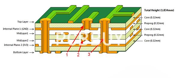
Dimensional Control in Multilayer PCBs
Copper clad laminate expansion and contraction must be controlled to maintain layer registration.
This is especially important for high-layer-count boards.

Manufacturing Challenges Related to Copper Clad Laminate
PCB manufacturers face several challenges when processing copper clad laminate:
-
Material variation between suppliers
-
Resin flow control in multilayer lamination
-
Warpage management after thermal processes
-
Compatibility with advanced PCB designs
Addressing these challenges requires both process control and engineering experience.
Process Controls Required for Reliable Copper Clad Laminate Handling
Effective PCB manufacturing relies on:
-
Incoming laminate inspection and qualification
-
Controlled lamination parameters
-
Optimized drilling and imaging conditions
-
In-process quality monitoring
These controls ensure consistent performance across different PCB projects.
PCBBUY’s Capability in Processing PCB Copper Clad Laminate
PCBBUY approaches PCB copper clad laminate processing with a focus on stability and repeatability. By working with qualified laminate suppliers and maintaining controlled production parameters, PCBBUY supports a wide range of PCB material requirements.
Key capability highlights include:
-
Experience with standard and high-Tg laminates
-
Stable multilayer lamination processes
-
Engineering support for material selection
-
Manufacturing aligned with export-quality standards
This allows PCBBUY to deliver reliable PCB products for global customers.

Design Considerations for PCB Copper Clad Laminate
Designers can improve manufacturability by:
-
Selecting laminate types appropriate for electrical and thermal needs
-
Considering material behavior during fabrication
-
Clearly specifying copper clad laminate requirements in design files
Early material planning reduces production risk and improves yield.
Typical Applications Using High-Quality Copper Clad Laminate
Reliable copper clad laminate is essential for:
-
Multilayer PCBs
-
High-speed and RF circuits
-
Industrial control electronics
-
Automotive and export-grade electronics
These applications demand consistent material performance and manufacturing precision.
Conclusion
PCB copper clad laminate forms the structural and electrical foundation of every printed circuit board. Its properties influence not only PCB performance but also manufacturing complexity and reliability.
By combining material knowledge with controlled manufacturing processes, PCBBUY ensures stable processing of copper clad laminate and delivers dependable PCB solutions to customers worldwide.
FAQ
What is PCB copper clad laminate?
PCB copper clad laminate is the base material used to manufacture printed circuit boards, consisting of copper foil bonded to a dielectric substrate.
Why is copper clad laminate important in PCB manufacturing?
It determines the PCB’s electrical insulation, thermal stability, mechanical strength, and overall manufacturing reliability.
What types of PCB copper clad laminate are commonly used?
Common types include standard FR-4, high-Tg laminates, high-frequency low-loss materials, and special-purpose laminates.
How does copper clad laminate affect multilayer PCB production?
Material stability affects layer alignment, lamination quality, drilling accuracy, and long-term PCB reliability.
What challenges exist when processing PCB copper clad laminate?
Challenges include resin flow control, warpage management, material variation, and compatibility with fine-line designs.
Can PCBBUY support special PCB copper clad laminate materials?
Yes. PCBBUY supports a range of copper clad laminate types and provides engineering guidance for material selection and processing.
Industry Category


