
PCB Copper Plating Thickness for Via Reliability: What Engineers Should Consider
By:PCBBUY 09/30/2026 16:47
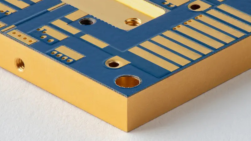
Copper plating is one of the most important manufacturing factors affecting the electrical and mechanical reliability of PCB vias. The plated copper forms the conductive path through a plated through-hole or blind via, but its function is not limited to electrical continuity. The copper structure must also withstand thermal expansion, assembly cycles, mechanical stress, and long-term operating conditions.
For this reason, PCB copper plating thickness for via reliability should not be evaluated as a single number. Plating thickness, via geometry, aspect ratio, copper distribution, material properties, and manufacturing consistency all interact to determine the reliability margin of the finished interconnect.
This is particularly important for automotive electronics, industrial control, power systems, energy storage, new-energy equipment, and other products where PCB interconnect failure can have significant consequences.
Why Does Copper Plating Thickness Affect Via Reliability?
A plated via contains a copper layer deposited on the internal surface of the drilled structure. During manufacturing and subsequent assembly, this copper experiences mechanical and thermal stresses.
When the PCB is heated, the laminate and copper expand at different rates, particularly in the Z-axis. Repeated thermal excursions can therefore place stress on the plated copper.
If the copper structure has insufficient thickness, poor uniformity, or defects at critical locations, the available mechanical margin can decrease.
For a plated through-hole, the barrel copper is particularly important because it must maintain electrical and mechanical continuity throughout the hole.
For an HDI microvia, the situation is more complex. The via is much shorter, but its geometry and the copper interface around the via bottom and target pad can become critical reliability locations.
More copper does not automatically mean a more reliable via.
The copper must be deposited uniformly and bonded properly to the surrounding structure.
PTH Via vs. Microvia: Copper Plating Is Not the Same
A common mistake during PCB specification is to use one copper-thickness requirement for every type of via.
PTHs and microvias have different geometries and manufacturing processes.
Plated Through-Hole (PTH)
A PTH passes through the PCB and creates a copper barrel connecting multiple conductive layers.
For PTHs, engineers should consider:
-
Finished hole diameter
-
Board thickness
-
Aspect ratio
-
Barrel copper thickness
-
Copper distribution
-
Thermal expansion
-
Current-carrying requirements
The copper thickness along the barrel is particularly important because the barrel may experience repeated mechanical strain during thermal cycling.
HDI Microvia
A microvia normally connects adjacent or selected build-up layers and is typically produced using laser drilling.
Its reliability depends on a broader process chain:
Laser drilling → desmear → surface preparation → copper deposition → electroplating → interconnection with the target pad
The plating process must establish a reliable conductive structure inside a much smaller geometry.
This is why simply specifying a very small laser via without considering plating and process margin can create unnecessary manufacturing risk.
What Factors Determine Via Reliability?
Copper plating thickness is important, but it is only one part of the reliability equation.
|
Factor |
Influence on via reliability |
|
Copper plating thickness |
Provides electrical and mechanical continuity |
|
Plating uniformity |
Prevents localized thin areas that can become weak points |
|
Via diameter |
Influences current capacity, geometry and manufacturing margin |
|
Aspect ratio |
Affects plating accessibility and copper distribution |
|
Target-pad structure |
Important for microvia electrical and mechanical connection |
|
Laminate Z-axis expansion |
Contributes to thermal-mechanical stress |
|
Registration |
Determines whether the via lands correctly on the intended structure |
|
Thermal cycling |
Repeated expansion and contraction can accumulate stress |
|
Manufacturing consistency |
Determines whether the design margin is maintained across production |
This is why a reliability-focused DFM review should consider the complete via structure, rather than asking only whether the specified copper thickness meets a nominal requirement.
Copper Plating Uniformity Matters as Much as Nominal Thickness
A manufacturer may specify a target plating thickness, but the actual copper distribution across a PCB is not necessarily identical everywhere.
Current density, board geometry, hole structure, copper distribution, and plating process conditions can all affect deposition.
For high-reliability applications, engineers should therefore distinguish between:
-
Nominal plating thickness
-
Minimum local thickness
-
Average thickness
-
Thickness distribution
-
Plating uniformity
PCBBUY uses microcrystalline phosphorus copper balls in its electroplating process and specifies electroplating uniformity of ≥97% within its stated heavy-copper process capability.
This is particularly relevant for boards where different areas contain substantially different copper densities.
How Heavy Copper Changes the Design Equation
Heavy copper introduces another dimension to via design.
PCBBUY supports up to 15 oz copper on outer layers and 8 oz on inner layers. This capability can be useful for high-current PCB structures used in power electronics, energy storage, new-energy systems, industrial control, and automotive power applications.
However, thick copper should not simply be applied everywhere.
Increasing copper thickness can affect:
-
Trace width and spacing
-
Etching requirements
-
Via connection design
-
Thermal behavior
-
Board weight
-
Layer balance
-
Manufacturing complexity
The via structure must therefore be designed together with the copper distribution of the entire PCB.
For example, a high-current power path may require heavy copper, while a nearby high-density signal section may need much finer geometry. The stackup and manufacturing process must accommodate both requirements.
HDI Microvias: Why Plating Quality Becomes Critical
As HDI structures become denser, microvia geometry becomes increasingly sensitive to manufacturing variation.
PCBBUY supports first-order and second-order HDI, with a minimum laser blind-via diameter of Φ0.075 mm and a minimum mechanical blind-via diameter of Φ0.15 mm.
The Φ0.075 mm figure is a manufacturing capability, not a recommended universal design size.
When engineers select a microvia, they should evaluate:
-
Laser via diameter
-
Dielectric thickness
-
Via depth
-
Target-pad size
-
Registration margin
-
Plating requirements
-
Stackup configuration
-
Reliability requirements
A smaller via can increase routing density, but it can also reduce the available manufacturing margin. The correct engineering objective is therefore not to minimize the via diameter, but to achieve the required density while maintaining an appropriate process window.
How Does Plating Relate to Thermal Reliability?
Thermal reliability is particularly important for automotive, power, and energy-related PCB applications.
During assembly and operation, the PCB can experience repeated temperature changes. The copper and laminate respond differently to these temperature changes because their material properties are different.
For PTH structures, this can place stress on the copper barrel.
For microvias, stress can be concentrated around the via geometry and copper interfaces.
The resulting reliability therefore depends on several linked variables rather than copper thickness alone.
This is why a high-reliability design should consider:
via geometry + plating quality + material selection + stackup + thermal environment + manufacturing consistency
rather than specifying an isolated copper-thickness value.
How PCBBUY Approaches Via Manufacturing
For advanced PCB projects, PCBBUY combines via fabrication with broader process capabilities instead of treating drilling and plating as independent operations.
Its manufacturing capabilities include:
-
First-order and second-order HDI
-
Minimum Φ0.075 mm laser blind vias
-
Minimum Φ0.15 mm mechanical blind vias
-
Up to 15 oz outer-layer copper
-
Up to 8 oz inner-layer copper
-
Electroplating uniformity ≥97%
-
Asymmetric and heterogeneous mixed-material lamination
-
AOI
-
Flying-probe testing
-
Four-wire low-resistance testingFor high-current designs, four-wire low-resistance testing can be particularly useful when low-resistance electrical paths are part of the customer's requirements.
For dense HDI structures, AOI and electrical testing can provide different forms of manufacturing verification. The exact inspection plan should be determined according to the board design and customer specification rather than applying one fixed test package to every PCB.
What Should Engineers Specify on the PCB Fabrication Drawing?
If via reliability is important to the product, the fabrication documentation should be sufficiently clear for the manufacturer to understand the intended structure.
Depending on the application, engineers may need to define:
-
Via type and finished hole requirements
-
Copper thickness requirements
-
Relevant minimum local thickness or applicable specification
-
PCB layer structure and stackup
-
Material requirements
-
HDI construction requirements
-
Surface finish
-
Electrical testing requirements
-
Inspection requirements
-
Any customer-specific reliability criteria
Avoid writing only “high-reliability vias” without defining what that means for the project.
The manufacturer needs measurable requirements that can be incorporated into engineering review and production control.
Conclusion
PCB copper plating thickness for via reliability is an important manufacturing consideration, but copper thickness alone does not determine whether a via will remain reliable.
For PTHs, barrel copper thickness, hole geometry, aspect ratio, material expansion, and thermal cycling all influence reliability. For HDI microvias, plating quality must also be considered together with laser geometry, target-pad connection, registration, dielectric thickness, and the overall build-up structure.
For high-reliability electronics, the most effective approach is to design the via structure around a realistic manufacturing process window rather than simply specifying the thickest possible copper or smallest possible via.
With first- and second-order HDI, Φ0.075 mm minimum laser blind vias, heavy-copper capability up to 15 oz on outer layers and 8 oz on inner layers, electroplating uniformity of ≥97%, mixed-material lamination, AOI, flying-probe testing, and four-wire low-resistance testing, PCBBUY can support PCB manufacturing requirements for automotive, industrial control, power and electrical systems, power supply, energy storage, new energy, and embodied robotics.
FAQ
1. Does thicker copper always make a PCB via more reliable?
No. Copper thickness is only one reliability factor. Plating uniformity, via geometry, aspect ratio, material expansion, registration, and thermal stress also affect the final interconnect.
2. Is copper plating thickness equally important for PTHs and microvias?
The principle is similar, but the failure mechanisms and geometry are different. PTH reliability is strongly related to barrel copper and thermal-mechanical stress, while HDI microvia reliability also depends heavily on the via geometry and copper interfaces around the target pad.
3. What is PCBBUY's heavy-copper capability?
PCBBUY supports up to 15 oz copper on outer layers and 8 oz on inner layers. The appropriate copper thickness should be selected according to current, thermal, mechanical, electrical, and manufacturing requirements.
4. What HDI microvia capability does PCBBUY provide?
PCBBUY supports first-order and second-order HDI, with a minimum laser blind-via diameter of Φ0.075 mm and a minimum mechanical blind-via diameter of Φ0.15 mm.
5. Why is plating uniformity important for via reliability?
A nominal copper thickness does not guarantee that the same thickness exists throughout the entire PCB or inside every critical via location. Good plating uniformity helps reduce localized thin areas that can become potential weak points.
6. Can heavy copper and HDI be used on the same PCB?
They can be combined when the stackup and manufacturing process are appropriately designed. The high-current regions and high-density regions may have very different copper and geometry requirements, so the complete board construction should be reviewed during DFM.
7. How should engineers specify via reliability requirements?
The fabrication documentation should define the relevant via type, geometry, copper requirements, material and stackup, inspection or testing requirements, and any customer-specific reliability criteria. A general statement such as “high reliability” is usually not sufficiently specific for manufacturing control.
Industry Category








