
PCB DFM Checklist for High Reliability Electronics: What Should Engineers Check?
By:PCBBUY 09/30/2026 16:29
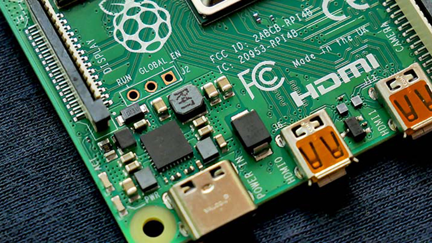
A PCB can pass an electrical design review and still create manufacturing problems if its geometry, materials, stackup, drilling, or inspection requirements are not aligned with the fabrication process.
This is why PCB DFM checklist for high reliability electronics should be treated as an engineering release procedure rather than a final visual check before sending Gerber files to a factory. For automotive electronics, industrial control equipment, power systems, energy storage, new-energy products, and embodied robotics, the objective is not simply to make the PCB manufacturable. The design should also provide sufficient process margin for repeatable production.
A good DFM review connects the PCB design with the manufacturer's actual process capabilities and the requirements of the finished product.

What Should a High-Reliability PCB DFM Review Cover?
A practical DFM review should start with the complete board construction rather than checking individual dimensions in isolation.
The following areas deserve particular attention:
-
Layer count and stackup
-
Material selection and dielectric structure
-
Copper thickness and current-carrying requirements
-
Trace width and spacing
-
Hole and via geometry
-
HDI and microvia structures
-
Registration and pad geometry
-
Solder mask and surface finish
-
Board outline and mechanical features
-
Copper distribution and warpage
-
Inspection and electrical testing
-
Fabrication notes and revision consistency
For high-reliability products, the key question is not whether one feature technically reaches a manufacturer's minimum capability. It is whether the overall design leaves adequate manufacturing margin.
1. Review the Stackup and Materials First
The PCB stackup determines much more than the number of copper layers. It affects impedance, dielectric thickness, thermal behavior, mechanical balance, via structures, and manufacturability.
Before fabrication, confirm:
-
Layer sequence and copper weights
-
Core and prepreg construction
-
Finished board thickness
-
Required electrical properties
-
Material compatibility
-
Symmetry or intentional asymmetry
-
HDI build-up structure where applicable
For high-speed or high-frequency sections, the material should be selected according to the actual electrical requirements rather than simply specifying a generic “high-frequency PCB.”
PCBBUY supports Rogers, TUC, Isola, and other high-frequency materials, as well as low-Dk/low-Df structures and asymmetric or heterogeneous mixed-material lamination.
This can be useful when a single PCB combines different electrical functions, but mixed-material construction should be reviewed before layout release because material compatibility and lamination behavior become part of the DFM equation.

2. Check Trace Width, Spacing, and Copper Weight
Trace geometry should always be evaluated together with copper thickness and the electrical function of the conductor.
A narrow signal trace and a high-current power trace cannot be evaluated using the same rule simply because both are “traces.”
For high-reliability electronics, check:
-
Minimum trace width
-
Minimum spacing
-
Copper thickness on each layer
-
High-current routing
-
Plane clearances
-
Thermal relief structures
-
Creepage and clearance where applicable
-
Controlled-impedance requirements
Avoid designing every feature exactly at the manufacturer's absolute minimum. A nominal capability is a manufacturing limit, not necessarily the preferred production target.
For power-intensive designs, PCBBUY supports heavy-copper structures with up to 15 oz outer-layer copper and 8 oz inner-layer copper. This provides additional options when high-current distribution must coexist with multilayer routing.
The final copper structure should still be determined from current, temperature rise, thermal design, board construction, and manufacturing requirements.
3. Review Drills, Vias, and HDI Structures
Drilling is one of the most important areas in a PCB DFM review because hole size, depth, registration, plating, and surrounding copper all interact.
The review should distinguish between:
-
Plated through holes
-
Non-plated holes
-
Blind vias
-
Buried vias
-
Laser microvias
-
Mechanical blind vias
-
Slots and special mechanical features
For HDI designs, PCBBUY supports first-order and second-order HDI. Its minimum laser blind-via diameter is Φ0.075 mm, while the minimum mechanical blind-via diameter is Φ0.15 mm.
These are manufacturing capabilities rather than universal design recommendations. If a design uses a Φ0.075 mm laser blind via simply because the factory can produce it, the engineering team may unnecessarily reduce its process margin.
Instead, via diameter should be evaluated together with pad size, dielectric thickness, layer registration, plating requirements, and the intended reliability level.

4. Check Registration and Pad Geometry
Registration becomes increasingly important as PCB geometry becomes smaller.
The DFM review should examine the relationship between:
-
Drill position and copper pads
-
Layer-to-layer registration
-
BGA pads and escape routing
-
Microvias and target pads
-
Solder mask openings
-
Board outline and copper features
PCBBUY's stated capabilities include pattern registration of ±3 mil and solder-mask offset of ±2 mil.
These figures should be used as manufacturing references during engineering review, not interpreted as permission to design every feature directly at the tolerance boundary.
For a high-reliability PCB, the objective is to leave enough geometric margin so that normal process variation does not turn into an open circuit, short circuit, insufficient annular ring, or soldering problem.
5. Review Copper Balance and Mechanical Stability
High-reliability DFM is not only about electrical connectivity.
Uneven copper distribution can influence lamination behavior and board flatness. Large copper areas next to relatively empty regions should therefore be reviewed during stackup and layout development.
This is especially important for:
-
Large multilayer boards
-
Heavy-copper designs
-
Boards with large power planes
-
HDI boards with uneven build-up structures
-
Boards containing large cutouts or mechanical features
Where required, PCBBUY supports customizable board warpage of ≤0.5%. The applicable requirement should be agreed according to the actual board construction and customer specification.

6. Review Solder Mask, Surface Finish, and Assembly Interfaces
The DFM review should not stop at copper geometry.
For fine-pitch components, BGA packages, connectors, and other dense SMT areas, check:
-
Solder mask openings
-
Mask registration
-
Pad-to-mask relationships
-
Surface finish
-
Component land patterns
-
Assembly clearances
-
Rework requirements where applicable
PCBBUY supports multiple surface finishes, including ENEPIG, ENIG, OSP, HASL, immersion gold, and immersion tin, as well as selective electroplated gold.
The correct surface finish should be selected according to the pad function, assembly process, storage requirements, and product requirements rather than simply choosing the most advanced-sounding finish.
7. Review Board Outline and Mechanical Features
A PCB can be electrically correct but mechanically difficult to manufacture.
Before release, verify:
-
Overall board dimensions
-
Slots and cutouts
-
Mounting holes
-
Edge clearances
-
Connector locations
-
Routing and milling requirements
-
Panelization assumptions
-
Board-edge copper
-
Warpage requirements
PCBBUY supports boards up to 1000 × 600 mm, with outline accuracy of ±0.05 mm.
For larger boards, the DFM review should pay particular attention to dimensional stability, registration, copper distribution, and the relationship between the PCB outline and the customer's mechanical enclosure.
8. Build Inspection and Testing Into the DFM Process
A high-reliability PCB should be designed not only to be manufactured but also to be inspected and electrically verified.
The inspection strategy should be established before production whenever possible.
PCBBUY supports:
-
AOI
-
Flying-probe testing
-
Four-wire low-resistance testing
The appropriate combination depends on the PCB structure and customer requirements.
For example, a dense HDI board may require detailed visual inspection of complex features, while a low-resistance power path may justify four-wire measurement. The important DFM principle is that the final design should provide a realistic path to verify the characteristics that matter to the product.

PCB DFM Checklist for High-Reliability Designs
|
DFM area |
What to check |
PCBBUY capability or consideration |
|
Stackup |
Layer order, dielectric structure, copper weights, material compatibility |
High-frequency materials and mixed-material lamination available |
|
Trace/space |
Minimum geometry relative to copper weight and process margin |
Confirm critical geometry during engineering review |
|
HDI |
Via diameter, pad size, dielectric thickness, registration |
1st/2nd-order HDI; laser blind via min. Φ0.075 mm |
|
Mechanical drilling |
Hole size, type, depth and positional requirements |
Mechanical blind via min. Φ0.15 mm; step-hole/slot positioning ±0.05 mm |
|
Copper |
Current capacity and copper distribution |
Up to 15 oz outer / 8 oz inner copper |
|
Registration |
Layer, drill, pad and solder-mask relationships |
Pattern registration ±3 mil; solder-mask offset ±2 mil |
|
Board size |
Outline, dimensional accuracy and mechanical interface |
Max. 1000 × 600 mm; outline accuracy ±0.05 mm |
|
Surface finish |
Finish matched to assembly and pad function |
ENEPIG, ENIG, OSP, HASL, immersion finishes, selective gold |
|
Inspection |
Visual and electrical verification |
AOI, flying probe, four-wire low-resistance testing |
What Should Be Checked Before Gerber Release?
A useful final DFM gate should confirm not only that the CAD design passes its internal DRC, but also that the manufacturing data is consistent.
Before release, verify:
-
The PCB revision matches the fabrication drawing.
-
Stackup information matches the actual design.
-
Copper weights are clearly defined.
-
PTH and NPTH holes are correctly identified.
-
Critical via structures are manufacturable.
-
Trace and spacing rules match the selected fabrication process.
-
Solder-mask and surface-finish requirements are clearly specified.
-
Board dimensions and mechanical features are consistent across files.
-
Special processes are clearly documented.
-
Inspection and electrical testing requirements are defined.
Passing an EDA design-rule check does not automatically mean that the PCB is ready for manufacturing. DRC checks the rules programmed into the design environment; DFM additionally asks whether those rules match the actual production process.
How PCBBUY Can Support DFM for High-Reliability Electronics
For high-reliability PCB projects, DFM works best when engineering review begins before production rather than after a manufacturing problem appears.
PCBBUY can support projects involving automotive, industrial control, power and electrical systems, power supply, energy storage, new energy, and embodied robotics. Its process capabilities cover conventional multilayer construction as well as HDI, heavy copper, high-frequency materials, mixed-material lamination, precision mechanical processing, and multiple inspection methods.
For a new project, engineers should provide the complete fabrication data package together with the intended stackup, material requirements, special processes, dimensional requirements, surface finish, and inspection requirements. The manufacturer can then evaluate critical features against the actual production route instead of applying generic DFM numbers to every PCB.

Conclusion
A PCB DFM checklist for high reliability electronics should be more than a list of minimum trace widths and hole sizes. It should verify that the complete design—materials, stackup, copper, vias, registration, mechanical structure, surface finish, inspection, and manufacturing documentation—fits within a realistic production window.
For demanding applications, designing at the absolute edge of a manufacturer's capability can unnecessarily reduce manufacturing margin. A better approach is to select the appropriate process capability first and then optimize the PCB geometry around that process.
With first- and second-order HDI, Φ0.075 mm minimum laser blind vias, heavy copper up to 15 oz on outer layers and 8 oz on inner layers, high-frequency and mixed-material lamination capabilities, precision mechanical processing, and AOI, flying-probe, and four-wire low-resistance testing, PCBBUY can provide engineering and manufacturing support for high-reliability PCB projects from DFM review through production and inspection.
FAQ
1. What is included in a PCB DFM checklist for high reliability electronics?
A comprehensive review normally covers stackup, materials, trace and spacing, copper thickness, drilling, vias, registration, solder mask, surface finish, board outline, mechanical features, inspection, testing, and manufacturing documentation.
2. Does passing PCB DRC mean the design is ready for manufacturing?
Not necessarily. DRC verifies the rules configured in the design software. DFM additionally checks whether those rules and the resulting geometry are compatible with the actual manufacturer's processes and production capabilities.
3. Should engineers design to the manufacturer's minimum capability?
Generally, a minimum capability should be treated as a process limit rather than an ideal design target. Leaving reasonable manufacturing margin can make production more robust, especially for complex or high-reliability boards.
4. What HDI capabilities does PCBBUY provide?
PCBBUY supports first-order and second-order HDI, with a minimum laser blind-via diameter of Φ0.075 mm and a minimum mechanical blind-via diameter of Φ0.15 mm. The appropriate via structure should be confirmed against the complete stackup and layout.
5. Can PCBBUY manufacture heavy-copper PCBs?
Yes. PCBBUY supports up to 15 oz copper on outer layers and 8 oz on inner layers. The actual copper thickness should be selected according to current, thermal, mechanical, and manufacturing requirements.
6. What inspection methods are available for high-reliability PCBs?
PCBBUY supports AOI, flying-probe testing, and four-wire low-resistance testing. The final inspection plan should be matched to the PCB design and customer requirements.
7. Which industries are suitable for PCBBUY's PCB manufacturing capabilities?
PCBBUY's capabilities are applicable to automotive, industrial control, power and electrical systems, power supply, energy storage, new energy, and embodied robotics, where controlled manufacturing processes and appropriate DFM planning are important.
Industry Category








