PCB Depaneling Stress on Solder Joints and Components
By:PCBBUY 10/29/2026 15:47
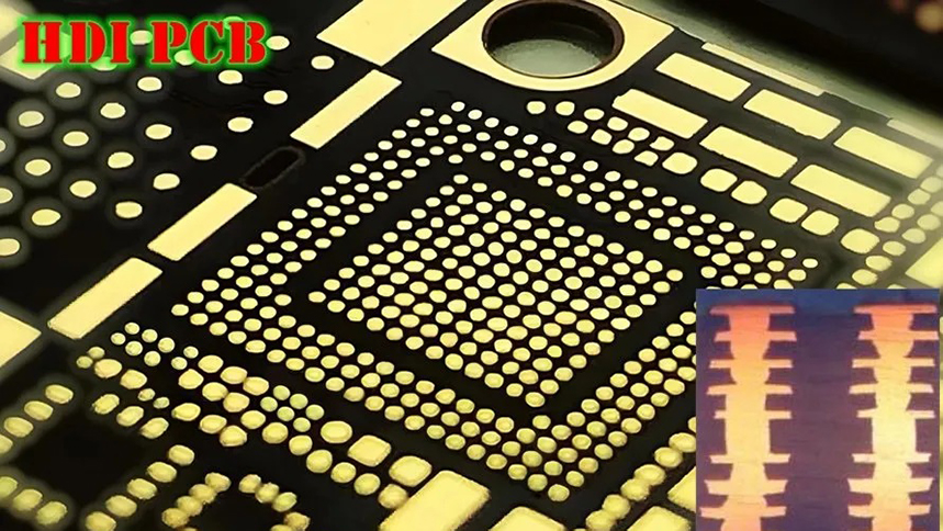
PCB depaneling is the process of separating individual printed circuit boards from a manufacturing panel after fabrication or assembly. Although this step may appear simple, excessive mechanical stress during separation can crack solder joints, damage ceramic capacitors, weaken copper pads, or create latent defects that are difficult to detect through visual inspection alone.
Understanding PCB depaneling stress on solder joints and components is particularly important for automotive electronics, industrial controllers, power conversion systems, energy-storage equipment, and robot control boards, where mechanical damage can affect long-term reliability. Effective prevention begins with panel design and continues through separation, inspection, and final shipment.
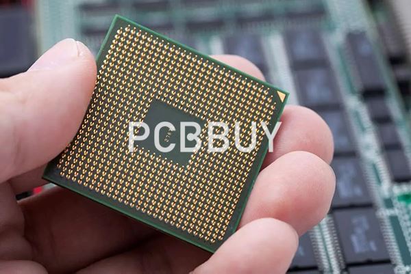
1. How Does Depaneling Stress Affect Solder Joints and Components?
Depaneling stress occurs when mechanical force bends, twists, or vibrates a PCB during separation. The resulting strain is transferred through the board to solder joints and mounted components.
Common risks include:
-
MLCC cracking: Multilayer ceramic capacitors are sensitive to board flexure. Mechanical stress can cause internal ceramic cracks, potentially leading to electrical failure.
-
Solder joint damage: Bending can initiate cracks in solder joints, especially around mechanically rigid components or areas experiencing concentrated strain.
-
Pad and trace damage: Excessive force near board edges or breakaway tabs may damage copper features or weaken local connections.
-
Latent reliability defects: Some cracks may not cause immediate electrical failure but can develop into intermittent faults during thermal cycling, vibration, or service life.
The risk depends on board thickness, material, component type, component location, separation direction, fixture support, and the depaneling method. No single method guarantees zero stress under all conditions.

2. Depaneling Methods and Their Mechanical Risks
|
Depaneling method |
Potential stress concern |
Recommended application |
|
Manual breaking |
Uncontrolled bending and sudden release of tabs |
Simple designs only when the risk has been evaluated |
|
V-scoring separation |
Bending stress concentrated along the score line |
Rectangular boards with straight separation edges |
|
Tab routing with mouse bites |
Localized stress around breakaway tabs |
Irregular PCB outlines and routed profiles |
|
CNC routing |
Tool vibration and local mechanical loading, depending on setup |
Complex outlines or designs requiring controlled cutting paths |
For assembled boards containing fragile components, a properly supported routing process may reduce bending compared with uncontrolled manual breaking. However, the actual result depends on equipment, fixture design, cutting parameters, and board construction. The process should be validated on the actual assembly rather than selected solely by its name.
3. Best Practices to Reduce PCB Depaneling Stress
3.1 Keep Sensitive Components Away from Separation Lines
Component placement is one of the most effective ways to reduce mechanical risk. Avoid placing fragile components directly beside V-scores, mouse-bite tabs, or routing paths whenever the layout permits.
Pay particular attention to MLCCs, fine-pitch packages, large connectors, and heavy components that may increase local mechanical loading. For MLCCs near a separation line, review both the component manufacturer's recommendations and the intended depaneling process. Orienting the capacitor's long axis parallel to the separation line can help reduce risk in some layouts, but it does not replace adequate clearance and process validation.
Copper features, exposed pads, and vias should also be positioned according to the manufacturer's edge-clearance rules.
3.2 Choose the Right Panelization Structure
V-scoring is often efficient for rectangular boards, while tab routing is more suitable for irregular outlines. The choice should account for component placement, board thickness, edge requirements, and how the assembled panel will be supported during separation.
For high-density industrial control boards, battery management systems, and robot controller assemblies, review the panel drawing together with the component placement data. A panel that is easy to manufacture may still be unsuitable for low-stress depaneling if sensitive components sit too close to the breakaway areas.
3.3 Use Suitable Fixtures and Controlled Separation
The board should remain adequately supported while the panel is separated. Avoid twisting the PCB, applying excessive hand force, or allowing an individual board to drop or rotate when its final connection is released.
For higher-risk assemblies, define the depaneling equipment, fixture support points, cutting sequence, and inspection method before production. Where required by the product's reliability plan, use strain measurement or other agreed validation methods to assess the actual process.
A universal strain limit should not be assumed. Acceptable limits need to come from the component manufacturer's guidance, customer requirements, applicable reliability criteria, or a validated product-specific process.
3.4 Validate the Process Before Volume Production
Run a pilot using representative assembled panels. Inspect components and solder joints near separation lines, and perform appropriate electrical or functional checks. For critical products, consider additional reliability evaluation based on the failure modes identified during engineering review.
If damage occurs, investigate the full process: panel design, component clearance, separation direction, tooling condition, fixture support, and operator handling. Changing only the depaneling machine may not solve a problem caused by poor component placement or unsuitable panel geometry.
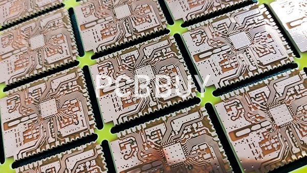
4. PCBBUY Manufacturing Review and Quality Control
PCBBUY's published PCB manufacturing capabilities include V-cut processing, routed board outlines, and manufacturing quality checks. Its documented V-cut parameters include residual-thickness control and a V-cut misregistration specification. Actual limits should be confirmed against the latest capability document and the specific board construction before design release.
For projects requiring reliable depaneling, the engineering review should consider:
-
Panel design: Confirm the separation method, board thickness, outline, and breakaway geometry.
-
Edge and copper clearance: Check sensitive components and copper features near the separation line.
-
Manufacturing feasibility: Verify V-cut or routing requirements against PCBBUY's applicable process capabilities.
-
Inspection planning: Define visual, dimensional, and electrical acceptance requirements appropriate to the product.
-
Assembly coordination: If the PCB will be populated by an SMT partner, agree on the depaneling method and validation responsibility with that assembly provider.
For projects in automotive electronics, industrial control, electricity, power supplies, energy storage, new-energy equipment, and embodied robotics, these checks help align PCB design decisions with the mechanical and reliability needs of the finished product.
Shipment Acceptance Checklist
|
Inspection item |
Acceptance consideration |
|
Board edges |
No unacceptable cracks, delamination, or mechanical damage |
|
Components near separation lines |
No visible cracking, chipping, or displacement |
|
Solder joints |
No observable damage or defects against the agreed inspection criteria |
|
Electrical performance |
Required continuity, isolation, and functional tests meet specifications |
|
Documentation |
Inspection and test records meet the order's agreed requirements |
|
Packaging |
Boards are protected against bending, impact, and handling damage during transit |
Visual inspection alone cannot rule out every latent solder-joint or component crack. For high-reliability assemblies, inspection and testing should be selected according to the product risk and customer requirements.
Conclusion
Reducing PCB depaneling stress on solder joints and components requires more than selecting a separation machine. Component placement, panelization geometry, fixture support, controlled separation, and product-specific validation all influence the outcome.
By reviewing these factors early and confirming manufacturing requirements with PCBBUY, design and sourcing teams can reduce avoidable mechanical damage and improve production consistency. For assembled boards used in automotive, industrial, energy, and robotics applications, coordinating PCB panel design with the assembly and depaneling process is essential to achieving reliable results.
FAQ
1. What causes PCB depaneling stress?
The main causes include board bending, twisting, vibration, excessive manual force, poorly positioned tabs, and inadequate fixture support during separation.
2. Which depaneling method produces the least stress?
There is no universally lowest-stress method for every PCB. Properly configured CNC routing can reduce board bending in suitable applications, while V-scoring and tab routing may be appropriate for other designs. The assembled product and actual equipment setup should be evaluated.
3. Can depaneling stress crack ceramic capacitors?
Yes. Mechanical strain can crack MLCCs, particularly when they are close to a separation line or mounted in a region that bends during depaneling. Adequate clearance, suitable orientation, and controlled separation reduce the risk.
4. How can solder-joint damage be detected after depaneling?
Start with visual inspection and appropriate electrical or functional tests. Depending on the package and failure risk, additional methods such as microscopy, X-ray inspection, or strain measurement during process validation may be useful. No single inspection method detects every possible mechanical defect.
5. Should depaneling requirements be included in the PCB fabrication drawing?
Yes. Specify the intended panelization and separation method, outline requirements, relevant clearances, and any special edge or mechanical constraints. For assembled boards, coordinate these requirements with the assembly provider and define additional validation criteria when needed.
Industry Category