PCB Design
By: 03/11/2021 10:57

PCB design is a main function in any electronic product development process. For a PCB to perform reliably and within its specification, the PCB design process is critical and must follow an effective process.
PCB Design Software
For both large companies and self-employed PCB board designers, there are many computer aided design (CAD) software packages available. The most commonly used CAD tools are Altium Designer, PADs, Allegro, and OrCAD. For students and hobbyists, there are free CAD tools available such as Eagle and KiCad, although their functionality is somewhat limited.
The PCB design software capabilities vary quite a bit. The basic software tools provide the simpler functions, while the pay-for tools enable more facilities such as complex routing and simulation. With the increased complexity and requirements in newer technologies, using a higher end software tool is often required.
Schematic Capture
Once a design specification is complete and creates a clear list of requirements for the PCB, the first stage is schematic capture. Although it is possible to draw a schematic manually, most schematics are captured on a computer using PCB design software. The schematic is a 2D rendering which serves as a blueprint for placing the components and laying out the traces on the PCB products. Schematic symbols are created and linked to a PCB footprint which defines each component’s physical dimensions and placement of the copper pads or through holes.
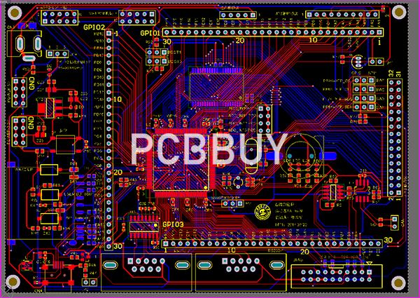
Component Placement
The next stage in PCB design is component placement. For components to be incorporated into the PCB design, they must have all of the relevant information defined in their footprints. Also, the board size and shape, any drilling information, keepouts, critical component locations, etc. must be defined.
Before getting into the detailed PCB design, it is important to get a rough idea of where the components will be located on the board and to determine if there is enough space on the board to contain all of the required circuitry. This process will also help determine how many layers will be needed. Once a rough placement has been completed, a more detailed component placement can begin. This can take into account things such as the proximity of devices that may need to communicate with each other or may affect the speed of certain signals, and other information such as RF considerations.

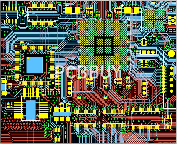
Routing
Once component placement is complete, the next stage of PCB design is to route the connections (traces) between all the components. First, if the design is more complex, a set of rules is input into the PCB design software which will trigger an error message if broken. Next, a netlist will be generated from the schematic, which shows all of the traces between all components. Critical routes are completed first, where size and length of the trace is critical. Then the remaining routes are completed, often moving up and down through multiple layers of the PCB.
Manufacturing Outputs
The information for the photo plots of the PCB design are output in the form of Gerber files. This is the standard format PCB manufacturers use and are a form of numerical control files used by a photo plotter. In addition to Gerber data, drill information is generated along with the screen print and photo-resist information. Pick and place data is generated, which manufacturers use to program the machines that actually affix the components to the PCB.
Industry Category


