PCB EMC Guidelines
By:PCBBUY 09/08/2021 09:44

Since PCB have strong performance to process in several products, it needs to have strong electromagnetic compatibility (EMC) built-in from the ground up. EMC is what keeps our devices from constantly interfering with each other. Now, EMC is more of an area of focus, and every PCB is expected to use these design practices to minimize unwanted emissions.
If you are going to learn more information about it, we will provide you everything about PCB EMC. Please check and read the content below for more knowledge.
If you want to order PCB product, please check and custom your order online.
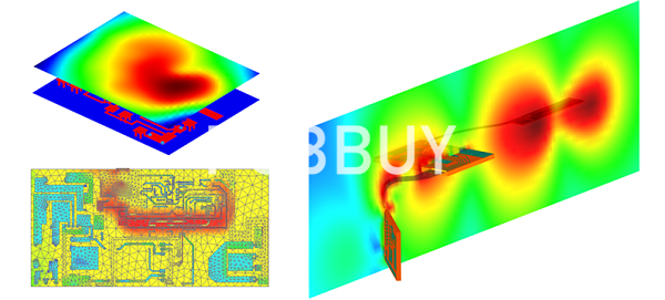
What is the importance of EMC test for PCB?
There are a number of good reasons why your boards should undergo testing for EMC; including the following:
Safety
The prevailing motivation for EMC testing is to ensure the safety of users and operators of the electronic equipment and systems of which your boards are a part.
Reliability
In addition to safety, boards should be tested to find out whether they will function as designed and meet their operational objectives within their deployment environment.
Regulations and Standards
Just in case the two reasons listed above do not provide the necessary motivation to perform EMC testing, then the fact that most EMC testing is mandatory and defined by one of many standards. From a regulatory perspective, only applicable testing must be done to avoid sanction(s) for noncompliance. Applicability may be determined by manufacturer location, end-user geolocation or industry for which the board is made.
How to design EMC for PCB?
Obviously, EMC compliance can be a major development issue depending upon the type of board you are building. In fact, for the more restrictive industries (aerospace, automotive, medical devices) noncompliance is synonymous with non-usable. Therefore, we know what EMC testing is and why it should be done. The last remaining question is whether you can aid the testing process during design. The answer is yes; however, the level of assistance is dependent upon the design tool you use.
Designing electronic systems for EMC can help you stay one step ahead by minimizing problems in the first place. Below are some EMC design techniques that you can implement to pass electromagnetic compatibility testing.
Board Layout
It is important to consider the signals that will be given off by your board. Some of these will be intentional, but 90% of electromagnetic interference (EMI) emissions from a PC board will be unintentional. Some of these unintentional signals are from common-mode currents, crosstalk coupling to I/O traces and power planes.
Lower frequencies look for the path of least resistance. They can be harder to find because they spread out more. Outgoing and return paths may be distant from each other in this case.
A few more general principles for controlling radiated emissions by design include the following.
· Increase traces width where possible. A wider trace size is shown to effectively decrease radiated emissions.
· One way to shield your inner layers from radiation is by filling your top and bottom layers with a solid ground plane and using ground-stitch vias throughout the PCB. Metalizing your PCB quote edges with copper plating may also help to decrease radiation from the inner layers and increase the cooling efficiency.
· Add stitching vias between your layers and near high-speed signal vias to keep current loops as small as possible.
· Avoid 90-degree angles if working with very high-speed applications.
Grounding
Poor grounding can be bad news for your EMC performance. It can lead to ground loops, resulting in radiated emissions or signals picked up from within the unit. Remember that a grounding system creates a path to return a current to its source. It needs to have low impedance and be as direct as possible.
· One way to help this process is to place a ground plane directly below the plane with your signal traces. This plane can shield against EMI. It offers low inductance and low resistance common ground, creating a short lead length to the ground. For some areas, you may need to isolate the ground so ground currents can't flow across the section.
· Never route signals over a split ground plane. Doing this can create large loops and high radiated emissions since the return current can't flow under or beside the forward current.
· The length of a grounding system should be kept to a minimum, to prevent inductance from becoming a problem. At low frequencies, this impact can become quite significant. Thick wires can help, as well as using ground planes with critical tracks on your PCB.
Industry Category


