PCB Edge Plating Guidelines Ensures High-Reliability Plating Quality
By:PCBBUY 11/19/2025 16:41
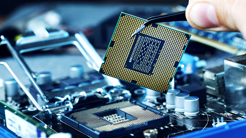
With the modern electronics, PCB edge plating is now an important characteristic used in high-density and high-reliability systems, where mechanical integrity and electrical characteristics are both important. With an increasing also of the number of designers using plated board edges as modular connector interfaces, EMI grounding features, and rugged interfaces, the proper PCB edge plating requirements are becoming an even more important issue.
At PCBBUY, we are leading in the state-of-the-art PCB production method, such as the full edge plating, castellated holes, and selective side plating of simple or complicated multi-layer boards. This paper provides a detailed instruction and emphasizes the ways our organizational manufacturing power contributes to making the customers gain uniform and dependable returns.
1. What Is PCB Edge Plating?
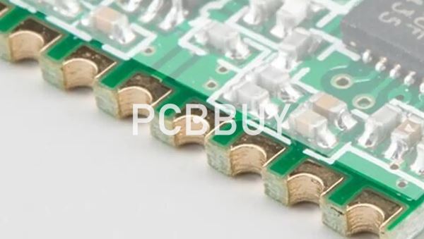
PCB edge plating—also known as side plating or edge metallization—is the process of applying copper along the perimeter of a PCB, or around castellated half-holes. This extension of copper to the board edge allows enhanced mechanical durability, improved conductivity, and high-strength connectivity for plug-in modules or board-to-board interfaces.

Common forms include:
-
Full edge plating (continuous copper on the entire PCB edge)
-
Castellated holes (partially drilled and plated half-holes)
-
Selective edge plating (localized side-wall copper for connectors or shielding)
Because edge plating requires additional CNC routing, custom plating fixtures, and controlled electroplating parameters, it is considered an advanced PCB manufacturing technique.
2. Why PCB Edge Plating Matters in Modern Designs
Following proper PCB edge plating guidelines matters for several reasons:
Mechanical Strength
Side plating reinforces the PCB structure, reducing wear during repeated insertion and removal.
Improved Electrical Performance
Plated edges provide a low-impedance path for grounding or joining modular connectors.
Enhanced EMI Shielding
Edge plating helps create a conductive enclosure around sensitive circuits.
Better Solderability for Modular Boards
In castellated modules, edge plating improves joint reliability when soldered onto a mother board.
For applications that require durability and stable electrical connections—such as RF modules, IoT devices, industrial sensors, and communication modules—edge plating is a crucial design feature.
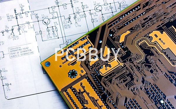
3. Essential PCB Edge Plating Guidelines for Designers
3.1 Copper Thickness Requirements
A successful edge plating design starts with proper copper thickness.
General recommendations include:
-
10–25 μm for standard applications
-
25–30 μm for high-reliability or high-current designs
PCBBUY can maintain plating accuracy within ±10%, even on complex multilayer builds.
3.2 Keep-Out Zones & Design Clearances
To avoid plating defects, the following PCB edge plating guidelines should be followed:
-
Maintain a safe clearance between copper features and the final board outline
-
Avoid tight copper-to-edge spacing to prevent plating buildup
-
Ensure solder mask openings do not overlap edge-plated areas
-
Provide accessible areas for plating racks and fixtures
PCBBUY's CAM engineers review each project to verify manufacturability before fabrication begins.
3.3 Mechanical Design Considerations
Edge plating interacts directly with routing processes. Designers should note:
-
CNC routing or milling quality directly affects plating adhesion
-
Avoid sharp corners on edge-plated areas
-
Maintain consistent spacing between the plated edge and inner copper layers
-
Use rounded or chamfered edges to reduce physical stress on the plating layer
PCBBUY uses high-precision routing equipment with ±0.05 mm tolerance, ensuring clean and uniform edges for copper deposition.
3.4 Castellated Hole Guidelines
For castellated modules, proper design is essential:
-
Half-hole diameter typically ranges from 0.4–0.8 mm
-
Copper plating inside the hole should be uniform to avoid breakage
-
Hole-to-hole distance must support reliable CNC milling
-
Prevent excessive plating thickness that may crack during singulation
PCBBUY employs specialized milling paths and reinforced plating strategies to prevent edge chipping or copper delamination.
3.5 Surface Treatment Compatibility
Edge plating is fully compatible with most surface finishes including:
-
ENIG
-
OSP
-
Immersion Tin
-
Immersion Silver
PCBBUY performs additional cleaning and micro-etching steps before plating to ensure excellent adhesion and uniformity.
4. PCB Edge Plating Manufacturing Workflow at PCBBUY
PCBBUY follows a strict and optimized fabrication sequence tailored to edge plating requirements:
-
Multilayer lamination and inner layer processing
-
Initial CNC routing or beveling of edges
-
Copper surface activation and roughening
-
Vertical or horizontal copper electroplating for side walls
-
Pattern plating, imaging, and etching
-
Surface finish application (ENIG/OSP/etc.)
-
Final routing, v-cutting, and mechanical finishing
-
Quality inspection: copper thickness, continuity, and adhesion
Our dedicated plating lines and custom fixtures ensure consistent results even on high-density multilayer PCBs.
5. PCBBUY’s Advanced Edge Plating Capabilities
To support global customers with demanding designs, PCBBUY offers:
-
Full, partial, and castellated edge plating
-
Precision copper thickness control
-
Special plating fixtures for complex board shapes
-
Up to 32-layer edge-plated stackups
-
Automated AOI and X-ray for hole wall inspection
-
Stress-relief routing to prevent delamination
-
High-volume capability with stable yield rates
We routinely produce edge-plated PCBs for RF modules, telecom devices, industrial equipment, consumer electronics, and automotive sensor modules.
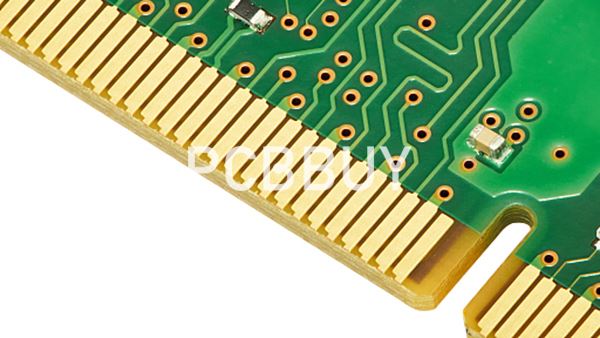
6. Applications That Benefit from PCB Edge Plating
Industries that rely on edge plating include:
-
RF communication modules
-
WeChat Mini-PC modules / IoT chipsets
-
Industrial signal conditioners
-
Vehicle sensors
-
Power modules with edge connectors
-
High-end consumer electronics
-
Wireless transceiver modules
-
Multi-board interface systems
PCBBUY supports both prototyping and mass production across all these sectors.
7. Why Choose PCBBUY for PCB Edge Plating Services?
Customers worldwide choose PCBBUY because we offer:
-
True one-stop PCB & PCBA manufacturing
-
Expert engineering support and free DFM files
-
Strict quality control with traceable records
-
Fast lead times for urgent R&D projects
-
Highly consistent batch production capability
-
Flexible options for custom plating and routing
Our engineering team ensures your design meets all necessary PCB edge plating guidelines while maximizing reliability and yield.
8. FAQ: PCB Edge Plating Guidelines
Q1: Does PCB edge plating affect solderability?
Yes—properly applied edge plating improves solderability, especially for castellated modules.
Q2: Can edge plating be combined with ENIG surface finish?
Absolutely. PCBBUY commonly produces ENIG + edge plating combinations for high-end modules.
Q3: What is the ideal copper thickness for edge plating?
Typically 10–25 μm, but high-strength interfaces may require up to 30 μm.
Q4: Do all PCBs require edge plating?
No—edge plating is recommended only for mechanical reinforcement, RF shielding, or connector interfaces.
Industry Category


