
PCB Impedance Mismatch Troubleshooting Guide
By:PCBBUY 07/24/2026 14:11
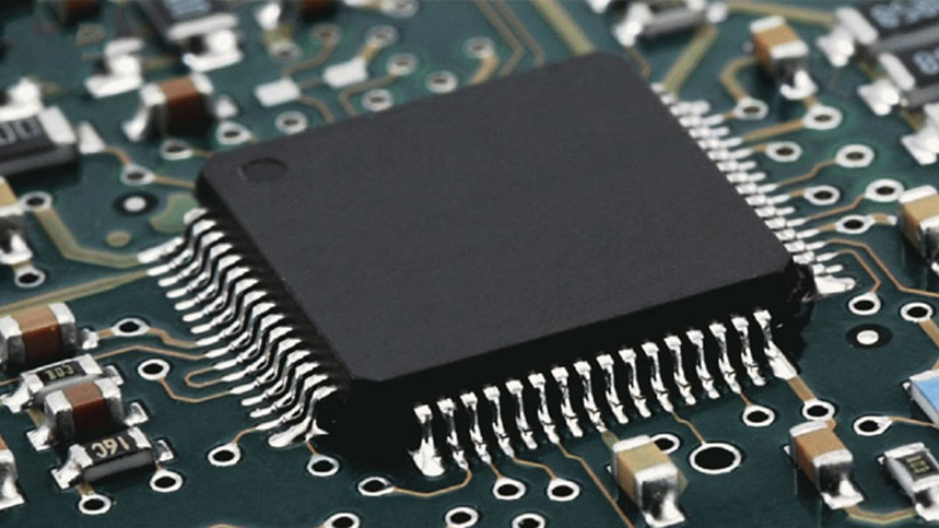
As signal frequencies continue to rise in applications such as 5G communications, AI servers, automotive electronics, high-speed networking, and industrial automation, maintaining accurate controlled impedance has become a critical requirement in PCB manufacturing. Even small impedance deviations can cause signal reflections, increased insertion loss, timing errors, and electromagnetic interference (EMI), ultimately affecting product performance and reliability.
This PCB impedance mismatch troubleshooting guide explains the most common causes of impedance mismatch, practical troubleshooting methods, and the manufacturing controls required to ensure consistent impedance performance. It also highlights how PCBBUY supports customers with precision controlled impedance fabrication and engineering services.
What Is PCB Impedance Mismatch?
Impedance mismatch occurs when the actual characteristic impedance of a PCB trace differs from its intended design value or when discontinuities exist along the signal path.
Typical controlled impedance values include:
-
50 Ω Single-Ended
-
75 Ω RF Transmission Lines
-
90 Ω Differential Pair (USB)
-
100 Ω Differential Pair (Ethernet, PCIe, LVDS)
-
85 Ω Differential Pair (DisplayPort)
When impedance is not properly controlled, part of the signal energy is reflected back toward the source instead of reaching the receiver.

Why Is Controlled Impedance Important?
High-speed digital and RF signals require predictable transmission characteristics.
Proper impedance control helps achieve:
-
Stable signal integrity
-
Lower insertion loss
-
Reduced signal reflection
-
Better eye diagram performance
-
Lower EMI emissions
-
Improved timing accuracy
-
Higher product reliability
For today's multi-gigabit interfaces, controlled impedance is no longer optional—it is a core design and manufacturing requirement.
Common Causes of PCB Impedance Mismatch
|
Cause |
Description |
Possible Impact |
|
Incorrect PCB Stackup |
Dielectric thickness differs from design |
Impedance deviation |
|
Trace Width Variation |
Manufacturing tolerance changes line width |
Reflection and signal loss |
|
Copper Thickness Variation |
Different copper weight affects impedance |
Impedance inconsistency |
|
Dielectric Constant (Dk) Variation |
Material properties differ from expected values |
Signal integrity degradation |
|
Poor Differential Pair Routing |
Uneven spacing or length mismatch |
Mode conversion and skew |
|
Incomplete Ground Reference |
Interrupted return path |
Increased EMI and reflection |
|
Via Discontinuities |
Excess via stubs or poor transitions |
Insertion loss and resonance |
Understanding the root cause is the first step toward effective troubleshooting.

How to Troubleshoot PCB Impedance Mismatch?
1. Verify the PCB Stackup
The PCB stackup determines:
-
Dielectric thickness
-
Copper spacing
-
Reference plane location
-
Controlled impedance geometry
Even small deviations in stackup can significantly affect impedance values.
Recommendation: Finalize the stackup together with your PCB manufacturer before routing begins.
2. Review Trace Geometry
Trace width and spacing directly influence impedance.
Designers should verify:
-
Trace width
-
Differential pair spacing
-
Copper thickness
-
Manufacturing tolerance
Simulation results should match the manufacturer's fabrication capability.
3. Check Material Selection
Different PCB materials have different dielectric constants.
|
Material |
Typical Dk Stability |
Recommended Applications |
|
Standard FR-4 |
Moderate |
General digital circuits |
|
High-Tg FR-4 |
Better |
Industrial electronics |
|
Rogers Materials |
Excellent |
RF and microwave designs |
|
Isola Low-Loss Laminates |
Excellent |
High-speed networking |
|
Hybrid Stackups |
Optimized |
Mixed RF and digital systems |
Selecting materials with stable dielectric properties improves impedance consistency.
4. Inspect Differential Pair Routing
For differential signals:
-
Maintain constant spacing.
-
Keep trace lengths matched.
-
Minimize unnecessary vias.
-
Route over continuous reference planes.
-
Avoid sharp corners.
These practices reduce skew and maintain differential impedance.
5. Evaluate Via Design
Vias introduce impedance discontinuities.
Optimization methods include:
-
Reducing via stubs
-
Using back-drilling when necessary
-
Employing blind or buried vias
-
Optimizing anti-pad dimensions
-
Maintaining consistent via geometry
Proper via design significantly improves high-speed signal performance.
6. Confirm Manufacturing Capability
Even a well-designed PCB may experience impedance mismatch if manufacturing tolerances cannot be achieved.
Key manufacturing controls include:
-
Precise line width control
-
Accurate dielectric thickness
-
Stable copper plating
-
Controlled lamination process
-
Impedance coupon testing
Working with an experienced PCB manufacturer minimizes these risks.
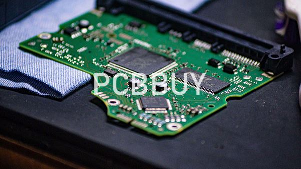
Manufacturing Factors Affecting Controlled Impedance
|
Manufacturing Parameter |
Impact on Impedance |
PCBBUY Control Method |
|
Trace Width |
Direct |
High-precision imaging and etching |
|
Copper Thickness |
High |
Stable electroplating process |
|
Dielectric Thickness |
High |
Controlled lamination process |
|
Material Dk |
High |
Certified laminate suppliers |
|
Layer Registration |
Medium |
Precision alignment equipment |
|
Etching Accuracy |
High |
Tight process control |
|
Stackup Consistency |
Critical |
Engineering verification before production |
Maintaining consistency across these parameters is essential for repeatable impedance performance.
PCBBUY Controlled Impedance Manufacturing Capabilities
PCBBUY provides comprehensive controlled impedance solutions for high-speed and high-frequency PCB applications.
|
Capability |
PCBBUY Specification |
|
PCB Layers |
1–26 Layers |
|
Controlled Impedance |
Single-Ended & Differential |
|
Minimum Line/Space |
35 μm (1.4 mil) |
|
Minimum Mechanical Hole |
0.10 mm |
|
HDI Capability |
1st–3rd Order HDI |
|
Material Options |
FR-4, High-Tg, Rogers, Isola, TUC, Halogen-Free |
|
Maximum Copper Thickness |
Up to 15 oz |
|
Engineering Support |
Stackup Design, DFM Review, Impedance Calculation |
|
Quality Inspection |
AOI, Flying Probe Test, X-ray Inspection |
|
Electrical Testing |
Impedance Coupon Verification Available |
Through advanced process control and engineering collaboration, PCBBUY helps customers achieve consistent impedance performance from prototype to mass production.
Best Practices for Preventing Impedance Mismatch
To reduce the risk of impedance mismatch:
-
Define impedance targets during schematic and stackup planning.
-
Use impedance simulation tools during PCB layout.
-
Select materials with stable dielectric properties.
-
Design balanced multilayer stackups.
-
Keep reference planes continuous.
-
Minimize unnecessary via transitions.
-
Collaborate with the PCB manufacturer before production.
-
Verify impedance through test coupons when required.
These practices improve first-pass success and reduce costly design revisions.

FAQ
Q1: What is the most common cause of PCB impedance mismatch?
The most common causes include incorrect stackup design, trace width variations, dielectric thickness changes, copper thickness inconsistencies, and routing discontinuities such as poorly designed vias.
Q2: How can impedance mismatch affect PCB performance?
Impedance mismatch can lead to signal reflections, insertion loss, degraded eye diagrams, increased EMI, timing errors, and reduced communication reliability in high-speed systems.
Q3: Can PCB manufacturers help optimize controlled impedance?
Yes. Experienced manufacturers work closely with customers to review stackups, calculate impedance, optimize fabrication parameters, and verify impedance using dedicated test coupons.
Q4: Are blind and buried vias better for impedance control?
In many high-speed applications, blind and buried vias help reduce via stubs and signal discontinuities, improving impedance continuity and overall signal integrity.
Q5: How does PCBBUY ensure controlled impedance accuracy?
PCBBUY combines engineering expertise, DFM review, optimized stackup design, precision imaging and etching, controlled lamination, stable plating processes, and impedance coupon verification to ensure reliable controlled impedance performance for demanding PCB applications.
Conclusion
A reliable PCB impedance mismatch troubleshooting guide begins with understanding that impedance accuracy depends on both good PCB design and precise manufacturing execution. Stackup planning, material selection, trace geometry, via optimization, and manufacturing consistency all play vital roles in maintaining signal integrity.
With capabilities including 1–26 layer PCB fabrication, controlled impedance processing, HDI technology, advanced material support (FR-4, High-Tg, Rogers, Isola, TUC), precision etching, impedance verification, and comprehensive DFM engineering services, PCBBUY provides end-to-end manufacturing solutions for high-speed, high-frequency, and mission-critical PCB applications. Whether developing AI computing platforms, automotive electronics, telecommunications equipment, industrial control systems, or aerospace products, PCBBUY helps customers transform impedance-controlled designs into high-quality, production-ready PCBs with confidence.
Industry Category








