
How Does PCB Laser Drilling Accuracy Affect Microvia Reliability?
By:PCBBUY 09/28/2026 15:50
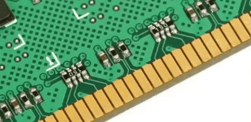
Laser drilling is one of the defining processes in HDI PCB manufacturing. Unlike conventional mechanical drilling, laser drilling creates very small blind vias by selectively removing dielectric material and exposing the underlying copper target pad.
As microvia dimensions become smaller, pcb laser drilling accuracy for microvia reliability becomes increasingly important. However, reliability cannot be determined by laser positioning alone. The final microvia structure also depends on dielectric thickness, laser energy, target-pad condition, registration, desmear, copper deposition, plating, filling, and lamination.
From an experienced PCB manufacturing perspective, the objective is therefore not simply to achieve the smallest laser via. It is to maintain a sufficient process window so that the microvia can repeatedly land on its target pad and form a stable electrical and mechanical interconnection.
1. Why Does Laser Drilling Accuracy Matter for Microvias?
A typical HDI microvia connects an outer or buildup layer to a nearby internal copper layer. The laser must remove the dielectric while exposing enough of the target pad for subsequent metallization.
If the laser position deviates from the intended location, several problems can occur:
-
Reduced contact area between the microvia and target pad
-
Partial breakout from the target pad
-
Insufficient copper landing area
-
Non-uniform plating conditions
-
Increased local electrical resistance
-
Greater mechanical stress at the microvia interface
This becomes particularly important in fine-pitch BGA fanout, where many microvias may be placed within a very small area.
However, laser accuracy should not be considered independently from PCB layer registration. The target pad itself may already have shifted because of imaging, lamination, material movement, or other manufacturing processes.
The actual landing margin is therefore determined by the combined process variation rather than the laser specification alone.
2. What Determines Laser Drilling Accuracy?
Several factors influence the final position and geometry of a laser-drilled microvia.
Laser Positioning
The laser must follow the programmed coordinates accurately. Equipment calibration, optical alignment, panel positioning, and compensation for dimensional changes can all affect the result.
Material Response
Different dielectric materials respond differently to laser energy. Resin content, glass reinforcement, dielectric thickness, and material composition can influence ablation behavior.
A laser recipe suitable for one material construction should not automatically be applied to another.
Panel Dimensional Stability
PCB materials experience dimensional changes during lamination and thermal processing. If the actual panel dimensions differ from the original CAD coordinates, the laser drilling position may require appropriate process compensation.
Target-Pad Alignment
Even when the laser reaches its programmed coordinate accurately, the microvia can still have insufficient landing margin if the underlying copper pad has shifted.
This is why HDI registration should be treated as a complete dimensional-control problem.

3. How Does Microvia Geometry Affect Reliability?
A microvia needs more than a correct center position. Its geometry must also provide a suitable surface for subsequent metallization.
Important characteristics include:
-
Via diameter
-
Via depth
-
Taper/profile
-
Bottom condition
-
Sidewall condition
-
Target-pad exposure
-
Position relative to the target pad
Excessive laser energy can damage the target copper or create undesirable thermal effects. Insufficient energy can leave dielectric residue at the bottom of the microvia.
Both conditions can interfere with subsequent copper deposition.
For this reason, the smallest possible laser aperture should not automatically be treated as the optimal engineering choice. A slightly larger microvia may provide greater process margin when the routing density allows it.
Lieban's stated HDI capability supports laser blind vias down to approximately Φ0.075 mm. This demonstrates the available process capability, but the appropriate production diameter should still be determined according to the actual stackup, dielectric thickness, target-pad geometry, routing density, and reliability requirements.
4. Why Is Desmear Important After Laser Drilling?
Laser drilling does not finish the microvia manufacturing process.
After dielectric ablation, residues can remain on the via wall or target-pad surface. These residues need to be properly removed before the conductive layers are formed.
If the surface is inadequately prepared, the subsequent copper layer may have a weak or inconsistent interface.
For microvia reliability, the process sequence can therefore be simplified as:
Laser drilling → cleaning/desmear → surface activation → copper deposition → plating/filling
Each step affects the next one.
This is one reason why a microvia that looks geometrically acceptable can still develop a reliability problem later. The critical interface may be hidden inside the finished PCB.
5. How Does Laser Accuracy Interact With Plating and Via Reliability?
After drilling and surface preparation, the microvia must be metallized.
A microvia that lands correctly but has poor metallization is not a reliable interconnection. Conversely, good plating cannot fully compensate for a microvia that has insufficient contact with its target pad.
The manufacturing relationship can therefore be viewed as:
Position accuracy + geometry + surface preparation + metallization = microvia interconnect quality
Potential defects include:
-
Incomplete copper coverage
-
Poor adhesion
-
Voids
-
Insufficient filling
-
Weak copper-to-target-pad interfaces
-
Cracks under thermal or mechanical stress
Microvia reliability research increasingly emphasizes the importance of the buried copper interfaces created during laser drilling, surface preparation, and metallization. This means that final electrical continuity alone may not reveal every latent reliability risk.
6. Why Is Registration Margin More Important Than the Nominal Laser Accuracy?
Consider a microvia designed to land near the center of a target pad.
The final position depends on multiple variables:
PCB dimensional change + layer registration + target-pad position + laser positioning + process compensation
If each feature is designed very close to its theoretical limit, relatively small variations can consume the available copper landing margin.
This is particularly important for:
-
Fine-pitch BGA packages
-
Stacked microvias
-
Small capture pads
-
High-density HDI routing
-
Multiple sequential lamination cycles
-
Via-in-pad structures
Therefore, engineers should design the target pad and microvia together with the PCB manufacturer's actual process window.
|
Manufacturing Variable |
Potential Effect on Microvia |
Engineering Response |
|
Laser positioning |
Via may shift from target center |
Maintain adequate target-pad margin |
|
Dielectric thickness |
Changes drilling depth and via profile |
Define stackup and pressed dielectric thickness carefully |
|
Laser energy |
Can cause incomplete ablation or target-pad damage |
Optimize process parameters for the material construction |
|
Lamination movement |
Changes layer-to-layer registration |
Include dimensional compensation and registration margin |
|
Desmear |
Affects surface condition before metallization |
Use an appropriate cleaning and activation process |
|
Copper plating |
Determines conductive connection quality |
Control deposition and filling according to via structure |
|
Via filling |
Affects stacked or via-in-pad structures |
Define filling requirements where applicable |
7. How Can Lieban Improve the Manufacturability of Laser-Drilled Microvias?
Lieban's HDI process supports first-order and second-order HDI structures, providing different options for dense interconnection designs.
Its stated laser blind-via capability reaches approximately Φ0.075 mm, while mechanical blind vias can reach approximately Φ0.15 mm. These capabilities can support dense BGA escape routing and compact interlayer connections when the complete PCB structure is suitable.
For more complex boards, Lieban also supports customized multilayer structures and asymmetric and heterogeneous mixed-material lamination. This can be relevant when microvias need to be integrated into boards containing different dielectric systems or demanding high-speed and power sections.
The engineering review should consider the complete relationship between:
-
Microvia diameter
-
Dielectric thickness
-
Target-pad dimensions
-
HDI order
-
Layer registration
-
Copper thickness
-
Filling requirements
-
Surface finish
-
Lamination sequence
Rather than automatically using the smallest available via, the preferred approach is to select a structure that satisfies the electrical and routing requirements while retaining reasonable manufacturing margin.

8. How Should Microvia Quality Be Verified?
Because microvias are internal structures, visual inspection of the finished PCB cannot reveal every possible defect.
Different inspection methods address different risks.
Lieban's stated inspection and testing capabilities include:
-
AOI for checking accessible PCB pattern features
-
Flying-probe testing for electrical verification
-
Four-wire low-resistance testing for more precise low-resistance measurement
For development or qualification work, cross-section analysis can also be useful for examining microvia diameter, profile, target-pad connection, plating condition, and layer registration.
The appropriate inspection plan should be determined according to the PCB structure, customer requirements, product application, and reliability expectations.
9. What Should Engineers Do Before Releasing an HDI Design?
The best opportunity to improve microvia reliability is before fabrication begins.
Engineers should provide the PCB manufacturer with:
-
Complete Gerber or equivalent fabrication data
-
Full layer stackup
-
Dielectric material and thickness information
-
Microvia diameter and depth requirements
-
Target-pad and capture-pad dimensions
-
HDI order and via structure
-
Via-filling requirements, where applicable
-
Copper thickness
-
Surface-finish requirements
-
Special registration or reliability requirements
A DFM review can then determine whether the proposed microvia geometry provides enough manufacturing margin.
This is particularly valuable for automotive, industrial control, power, energy-storage, new-energy, and embodied-robotics products, where an HDI structure may need to operate reliably under demanding thermal and mechanical conditions.

Conclusion
PCB laser drilling accuracy for microvia reliability is not simply a question of how precisely a laser can follow a programmed coordinate. Reliable microvias result from controlling the complete manufacturing chain.
Laser positioning must work together with material selection, dielectric thickness, layer registration, target-pad geometry, laser energy, desmear, copper deposition, plating, filling, and lamination.
Lieban's ability to manufacture first-order and second-order HDI structures, laser blind vias down to approximately Φ0.075 mm, and customized multilayer PCB structures provides a foundation for dense microvia applications. Its AOI, flying-probe, and four-wire low-resistance testing capabilities further support manufacturing and electrical verification.
The practical engineering objective should always be sufficient process margin rather than minimum geometry alone. When the microvia structure is designed around the actual fabrication process, laser-drilling capability can be converted into consistent HDI interconnect performance and more reliable production.
FAQ
1. Why is laser drilling accuracy important for microvia reliability?
Laser positioning determines where the microvia lands on its target pad. Excessive positional deviation can reduce the available copper connection area and increase the risk of breakout or a weak interconnection.
2. Does a smaller laser-drilled microvia always provide better performance?
No. A smaller microvia can increase routing density, but it also provides less manufacturing margin. The diameter should be selected according to the routing requirement, dielectric thickness, target-pad structure, and manufacturing capability.
3. What is Lieban's minimum laser blind-via capability?
Lieban's stated capability supports laser blind vias down to approximately Φ0.075 mm. This is a manufacturing capability rather than a universal recommended design value.
4. Can accurate laser drilling alone guarantee microvia reliability?
No. Laser accuracy is only one part of the process. Layer registration, dielectric behavior, desmear, copper deposition, plating, filling, and lamination can also affect the final microvia.
5. Why is the target pad important for laser-drilled microvias?
The laser-drilled via needs sufficient copper overlap with the target pad to create a reliable interconnection. If registration variation consumes too much of the available pad area, the resulting connection may have reduced mechanical and electrical margin.
6. What information should be provided for a microvia DFM review?
The manufacturer should receive the complete stackup, material construction, microvia dimensions, target-pad dimensions, HDI order, copper thickness, via-filling requirements, surface finish, and fabrication data. Reviewing these elements together allows the manufacturer to evaluate the actual process margin before production.
Industry Category








