
What Are the PCB Manufacturing Challenges for Fine-Pitch BGA Packages?
By:PCBBUY 09/28/2026 14:49
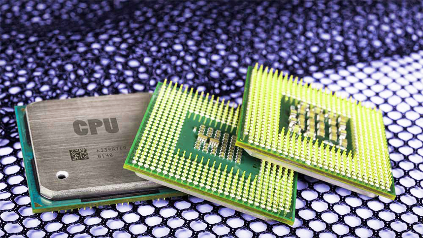
Fine-pitch BGA packages provide a high number of electrical connections within a relatively small PCB area. As the ball pitch decreases, however, the available space for pads, traces, vias, and solder-mask dams becomes increasingly limited. This makes pcb manufacturing challenges for fine pitch bga packages significantly different from those of conventional BGA designs.
The challenge is not simply making smaller features. A reliable fine-pitch BGA PCB requires sufficient manufacturing margin between multiple processes, including imaging, etching, drilling, laser via formation, lamination, plating, solder-mask application, and surface finishing.
For applications such as automotive electronics, industrial control, power equipment, energy storage, new-energy systems, and embodied robotics, this becomes particularly important because dense BGA interconnects may need to coexist with high-current power paths, high-speed signals, thermal structures, and demanding reliability requirements.
1. Why Are Fine-Pitch BGA Packages Difficult to Manufacture?
A BGA package becomes increasingly sensitive to PCB manufacturing variation as its pitch decreases.
At a relatively large pitch, there may be enough room to place a conventional fanout trace and via outside each pad. With a finer pitch, the same approach may no longer provide sufficient routing space.
Several manufacturing tolerances then begin to interact:
-
Copper pad dimensions
-
Trace width and spacing
-
Via diameter and capture-pad size
-
Layer-to-layer registration
-
Solder-mask registration
-
Solder-mask opening and dam width
-
Surface-finish thickness
-
Lamination movement
-
Drill or laser-via positioning
A design may therefore appear manufacturable in CAD while having very little process margin in actual production. This is why early DFM review is particularly valuable for fine-pitch BGA designs. Industry experience also shows that solder-mask misregistration can expose adjacent copper or vias in dense BGA areas and increase the risk of solder bridging.
2. How Does BGA Pad and Solder-Mask Design Affect Manufacturing?
BGA pad geometry must be considered together with solder-mask capability.
For fine-pitch packages, there is a limited amount of space between adjacent pad openings. If the solder-mask opening is too large or the mask shifts relative to the copper pattern, the available isolation between neighboring pads can become insufficient.
This can contribute to:
-
Solder bridging
-
Exposed adjacent copper
-
Inconsistent solder-pad definition
-
Reduced assembly margin
-
Difficult inspection and troubleshooting
The exact pad and solder-mask dimensions should therefore be determined from the BGA component manufacturer's land pattern, PCB fabricator's capabilities, and assembly process requirements, rather than applying one universal dimension to every fine-pitch package.
For particularly dense BGA areas, the PCB manufacturer should receive the package pitch and recommended land pattern during engineering review so that the pad, mask, and escape structure can be checked together.

3. Why Is BGA Escape Routing a Major Manufacturing Challenge?
Escape routing is often one of the first limitations encountered in fine-pitch BGA design.
With conventional through-hole vias, the via pad occupies considerable PCB area. As the BGA pitch decreases, there may not be enough space between adjacent pads for a conventional trace-and-via fanout.
Designers may then consider:
-
Microvias
-
Blind vias
-
Via-in-pad
-
HDI structures
-
Sequential buildup
-
Alternative layer assignments
The appropriate solution depends on the actual package geometry and required number of escape layers.
The important point is that the smallest possible via is not automatically the best via. Smaller geometries reduce routing space requirements but also reduce manufacturing margin for drilling, registration, plating, and filling.
4. How Do Microvias and Via-in-Pad Affect Fine-Pitch BGA Manufacturing?
HDI technology can significantly improve routing flexibility around fine-pitch BGAs.
A laser microvia can connect an outer-layer BGA pad to a nearby inner layer without requiring the larger footprint of a conventional through-hole via. For very dense packages, microvia-in-pad structures can provide an even more direct escape route.
However, via-in-pad introduces additional process requirements.
The manufacturer may need to control:
-
Laser-via diameter and depth
-
Capture-pad geometry
-
Via-to-pad registration
-
Via filling
-
Copper plating
-
Surface planarization
-
Lamination alignment
An improperly filled via inside a solder pad can create solder-volume variation or solder wicking during assembly. Therefore, via-in-pad should be specified according to the qualified fabrication process rather than being selected only for routing convenience.
PCBBUY supports first-order and second-order HDI structures, with laser blind vias down to approximately Φ0.075 mm and mechanical blind vias down to approximately Φ0.15 mm, subject to the complete PCB structure and manufacturing requirements.
This capability can provide additional flexibility when fine-pitch BGA fanout requires HDI technology.
5. How Does Layer Registration Affect Fine-Pitch BGA Reliability?
Fine-pitch BGA structures are sensitive to cumulative registration errors.
The relevant relationships include:
BGA pad ↔ microvia ↔ inner-layer trace ↔ reference plane
If these features are not sufficiently aligned, the available copper landing margin can be reduced.
This becomes especially important for:
-
Small microvia capture pads
-
Stacked or sequential microvias
-
High-density BGA fanout
-
Thin dielectric structures
-
Multiple HDI buildup layers
For this reason, the PCB stackup should be designed around the manufacturer's qualified registration capability. Reducing pad dimensions simply to gain routing space can be counterproductive if it leaves insufficient process margin.
6. What Other PCB Manufacturing Issues Should Be Considered?
Fine-pitch BGA manufacturing is not limited to HDI and solder-mask registration. Several other PCB processes can affect the final result.
|
Manufacturing Factor |
Fine-Pitch BGA Risk |
Engineering Consideration |
|
Pad geometry |
Insufficient soldering margin |
Follow component land-pattern requirements and fabricator DFM rules |
|
Solder-mask registration |
Pad exposure or solder bridging |
Provide sufficient mask clearance and registration margin |
|
Microvia positioning |
Partial capture or breakout |
Match via geometry to the manufacturer's qualified process |
|
Via filling |
Solder wicking or uneven pad surface |
Define via-in-pad filling and planarization requirements where needed |
|
Layer registration |
Misalignment between via, pad, and trace |
Review HDI buildup and stackup together |
|
Surface finish |
Variation in pad surface condition |
Select a finish compatible with the component and assembly process |
|
PCB warpage |
Uneven assembly conditions |
Balance stackup and copper distribution |
|
Inspection |
Hidden BGA joints are difficult to inspect visually |
Establish appropriate electrical and assembly inspection methods |
These factors are interconnected. For example, a smaller BGA pad may provide more routing space but leave less room for a microvia landing area. A larger solder-mask opening may improve solder exposure but reduce the mask dam between adjacent pads.
The correct solution is therefore a coordinated DFM decision rather than optimizing one parameter independently.

7. How Can PCBBUY Support Fine-Pitch BGA PCB Manufacturing?
PCBBUY's capabilities are particularly relevant when a fine-pitch BGA design requires HDI, dense multilayer routing, or special via structures.
Its HDI manufacturing supports first-order and second-order structures, with laser blind vias down to approximately Φ0.075 mm. Mechanical blind vias can reach approximately Φ0.15 mm. These capabilities can be used to support compact BGA escape structures when the package geometry and stackup require them.
For boards that combine fine-pitch BGA devices with high-current sections, PCBBUY also supports heavy and partial-heavy copper. Its stated capability reaches up to 15 oz copper on outer layers and 8 oz on inner layers, subject to the specific board structure and process conditions.
This can be useful for products where a dense digital/control section and a power section need to coexist on the same PCB.
PCBBUY can also manufacture boards up to approximately 1000 × 600 mm, which provides flexibility for larger industrial, power, energy-storage, and system-level control boards.
On the inspection side, PCBBUY uses processes including AOI, flying-probe testing, and four-wire low-resistance testing. These provide different levels of verification for fabricated copper patterns and electrical connections.
For fine-pitch BGA projects, however, the most important step remains engineering review before production. The Gerber files should be accompanied by the BGA package information, stackup, via specifications, solder-mask requirements, surface finish, and any special manufacturing notes.
8. How Can Engineers Reduce Fine-Pitch BGA Manufacturing Risk?
The most effective approach is to involve the PCB manufacturer before the layout is completely locked.
A practical review should examine:
-
BGA pitch and land pattern — Confirm the PCB footprint against the component manufacturer's requirements.
-
Escape strategy — Determine whether conventional vias, blind vias, microvias, or via-in-pad are appropriate.
-
Solder-mask structure — Check whether the required openings and dams provide adequate fabrication margin.
-
HDI stackup — Verify that the proposed buildup structure is compatible with the intended microvia geometry.
-
Via filling — Define filling and planarization requirements when vias are located in solder pads.
-
Registration margin — Avoid designing features at the absolute limit of manufacturing capability.
-
Copper distribution — Consider power, thermal, and mechanical requirements alongside BGA routing.
-
Inspection requirements — Define how critical fabrication features and electrical connections will be verified.
This early collaboration is especially valuable for automotive, industrial-control, power, energy-storage, new-energy, and embodied-robotics products, where PCB reliability and production consistency can be as important as routing density.

Conclusion
The main pcb manufacturing challenges for fine pitch bga packages come from shrinking geometries and increasingly limited manufacturing margin. Pad dimensions, solder-mask registration, microvias, via-in-pad structures, layer registration, surface finish, and board flatness must all work together.
Fine-pitch BGA manufacturing should therefore begin with a realistic DFM strategy rather than simply pushing individual dimensions toward their minimum values.
For applications requiring dense BGA escape routing, PCBBUY's first-order and second-order HDI capability, laser blind vias down to approximately Φ0.075 mm, heavy and partial-heavy copper processing, multilayer fabrication, and electrical inspection capabilities provide a manufacturing foundation for demanding PCB structures.
The final design should always be evaluated against the actual package footprint, stackup, materials, via structure, and manufacturer's qualified process window. This is the most reliable way to convert a fine-pitch BGA layout from a theoretically routable design into a PCB that can be manufactured consistently.
FAQ
1. What makes fine-pitch BGA PCBs difficult to manufacture?
The main difficulty is the limited space between adjacent pads and the small manufacturing margin available for traces, vias, solder-mask openings, and layer registration. As pitch decreases, normal fabrication variation becomes more significant.
2. Do fine-pitch BGA packages always require HDI?
No. The required technology depends on the BGA pitch, package size, I/O count, escape routing requirements, and available PCB layers. HDI becomes increasingly useful when conventional through-hole fanout cannot provide sufficient routing space.
3. What is the benefit of microvias for fine-pitch BGA packages?
Microvias occupy less routing area than conventional through-hole vias and can connect BGA pads to nearby inner layers. This can create additional escape-routing options in dense BGA regions.
4. Why is solder-mask registration important for fine-pitch BGA?
As the spacing between BGA pads decreases, a small mask-to-copper positional shift can consume the available isolation between adjacent openings. Poorly controlled registration can therefore increase the risk of exposed copper or solder bridging.
5. Can PCBBUY manufacture HDI PCBs for fine-pitch BGA packages?
PCBBUY supports first-order and second-order HDI structures, including laser blind vias down to approximately Φ0.075 mm and mechanical blind vias down to approximately Φ0.15 mm, subject to the specific stackup and manufacturing requirements.
6. What information should I provide when requesting a fine-pitch BGA PCB quotation?
Provide the Gerber files, BGA package pitch and land pattern, layer count, proposed stackup, material requirements, copper thickness, via specifications, solder-mask requirements, surface finish, board dimensions, and any special reliability or assembly requirements. Complete information allows the manufacturer to conduct a more meaningful DFM review before production.
Industry Category








