PCB Pad Size Guidelines with 5 Basic PCB Layout Tips
By:PCBBUY 09/27/2021 09:50

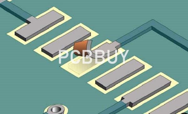
A pad is the exposed region of metal on a circuit board that the component lead is soldered to. Multiple pads in conjunction are used to generate the component footprint or land pattern on the PCB. The two types of pads available are through-hole and surface mount pads.
In this article, we will focus on the PCB pad size and the tips during the PCB layout process. In you are interested in PCB pad size, please check and read the content for more professional knowledge for more information.
What are the 5 tips for PCB pad size in PCB layout?
1. The standard of PCB pad size
Here are the design standards of PCB Pad shape and size:
The PCB Standard Packaging Library should be used.
· All pads should have a minimum of 0.25mm unilateral and a maximum total pad diameter not greater than 3 times the aperture of the part.
· It is important to ensure that the distance between the two pads is greater than 0.4mm. In the case of dense wiring, the recommended oval and oval plate. Single-panel pad diameter or minimum width of 1.6mm; weak-sided double-sided circuit board pad diameter hole diameter plus 0.5mm can be too large pad easily lead to unnecessary welding.
· Pads with a hole diameter of more than 1.2 mm or with a pad diameter of more than 3.0 mm should be designed as diamond or plummet pads
· For the plug-in components, in order to avoid the phenomenon of copper foil broken when welding, and the single side of the copper foil with a completely coated; and double-sided minimum requirements should make up the tear drop.

2. The calculator of PCB pad size
Many years ago PCB designers had to create their footprints using information from data sheets along with general pad and land size formulas. This was error prone and not always consistent with current data for all PCB fabrication and manufacturers. Fortunately, there is more error-free and productive options available to you these days.
One such option would be to register with a company that specializes in creating footprints for the specific CAD tools that you use. They have many years of experience doing this kind of work and can be very cost-effective in saving you the time needed for footprint research and development. Another option is to use a land pattern calculator. You can find these online and they will help you to create land patterns and footprints according to the latest available standards.
3. Get into know the types of pad in PCB layout
A pad may consist of several different shapes and styles. Normally two types of PCB pads are used, usually including a soldered surface-mount pad or a soldered thru-hole pad. A surface mount pad is a square or rectangular copper area used for mounting surface-mount components, its size and shape depend on the component soldered to the pad.
PLTH and NPTH
While the soldered thru-hole pad includes a plated thru-hole pad (PLTH) or a nonplated thru-hole pad (NPTH).Both are a round, square, or oblong pad with a hole through the pad. This makes a leaded component to be mounted to the board by placing the lead through the hole and the lead soldered to the pad area. The difference between the two kinds of soldered thru-hole pads is whether the hole is plated or not.

4. Issues of PCB pad size in PCB layout
Here are some examples of those problems:
Floating parts: If a surface mount part is sitting on pads that are too large or spaced incorrectly, the part may float out of position during solder reflow. This can lead to the solder bridging over to other metal and insufficient component spacing for thermal cooling, rework, and PCB test.
Incomplete solder joints: Pads that are too small or spaced too closely together may not allow enough room for a sufficient solder fillet to form. This can leave the part with a bad solder connection or no solder joint at all.
Solder bridging: As we discussed above, surface mount pads that are too large can allow a part to float, which could lead to solder bridging. This is where the solder crosses over to a pad or metal feature on another net and creates a direct short. Solder bridging can also happen if the correct solder mask and solder paste features are not designed into the pad shape in the CAD tools.
Tombstoning: When a small, discrete surface mount part is thermally unbalanced during solder reflow, the solder paste on one pad may melt faster than on the other and pull the part up in a vertical, or “tombstone,” position. This is usually the fault of one pad being connected to a large metal plane that acts as a heat sink, but it can also happen if inconsistent pad sizes are used between the two pins.

5. Learn to know the importance of PCB pad size in PCB layout
First of all, let’s define exactly what a “pad” is. A pad, also known as a “land,” is the exposed area of metal on a circuit board that the lead of a part will be soldered to. Multiple pads are used to create the component footprint, or land pattern, on the printed circuit board.
For through-hole parts, the pad is usually round in shape and will have a plated hole going through it for a component lead to be inserted into and soldered. For surface mount technology (SMT) parts, the pad will vary in size and shape depending on the component to be soldered. Sometimes, there are unusual sized and shaped pads for thermal or mechanical reasons, and small round pads are usually used for registration and alignment by automated optical equipment.
Industry Category


