PCB Pad Size Standards
By:PCBBUY 08/27/2021 10:09

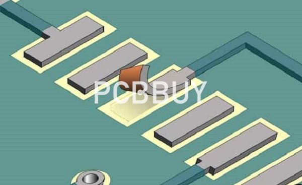
Do you know what PCB Pad is? In short, a PCB pad is the exposed PCB surface where components are mounted and soldered. On a printed circuit board, the pad that a component will solder to plays a similar role in that its purpose is to provide a stable foundation for the part. Incorrect sizes, alignments, or locations of the pads can cause problems for the component in both its electrical performance and its manufacturability. To avoid these problems, it is important to use acceptable PCB pad size guidelines in the construction and placement of pads and their associated footprints.
In this article, we are going to tell you everything about PCB Pad size. If you are interested in it, want to learn more about PCB professional knowledge. Please check and read the content below.
Why PCB Pad size standards are important?
First of all, let’s define exactly what a “pad” is. A pad, also known as a “land,” is the exposed area of metal on a circuit board that the lead of a part will be soldered to. Multiple pads are used to create the component footprint, or land pattern, on the printed circuit board.
This process could be very error-prone, however, as manufacturers’ specifications didn’t always adhere to the same formulas. This could result in layout designers using the wrong sizes and shapes in their pads. These incorrect pad sizes and shapes, unfortunately, could have disastrous consequences during manufacturing, including:

· Through-hole breakout: Through-hole pads must have a solid annular ring for solderability, which is the metal between the hole wall and the outer perimeter of the pad. The annular ring specification is designed to be large enough to allow for the expected amount of drill wandering from the center of the hole. If the pad is too small, however, there could be some breakout of the annular ring, and too much breakout can result in improper soldering or broken and incomplete circuits.
· Insufficient solder joints: SMT parts that have too small of pads run the risk of not getting a proper solder fillet during manufacturing. Without a good fillet, the solder joint will be weak and can break.
· Floating parts: SMT parts that are soldered to pads that are too large could end up floating out of position during solder reflow. This can cause conflicts with other parts or even shorts between circuits.
· Tombstoning parts: Smaller two pinned SMT parts, like resistors and capacitors, can have problems soldering if their pads are not the same size. One pad will heat faster than the other, and the melting solder will pull the part up and away from the other pad, sticking up like a tombstone.
· Shorts to other metal: Pads that are too small will allow surface traces too close to the parts that are soldered onto them creating potential areas of metal shorting together. On the other hand, pads that are too large could restrict trace routing between them, making it more difficult to route the board.

What are the guidelines of PCB Pad size?
There are several different resources available for getting the correct sizes and shapes of the PCB pads and component footprints that you will be working with. Here are a few that you can look into for finding the specifications that you need:
Industry standards
The PCB design industry has developed standards over the years for every aspect of circuit board layout, including recommended pad and land pattern sizes. IPC-7351 is an example of one of these, and there are others as well.
Component vendor data sheets
Each PCB component manufacturer will publish a data sheet on the parts that they provide. In addition to the electrical and physical specifications in these data sheets, they often will include a recommended PCB layout land pattern as well.
Corporate standards
Many companies have their own pad land pattern standards that they expect to be followed in the design of their circuit boards. These footprints are usually a combination of industry standards and vendor specifications tailored for their specific PCB manufacturers.
PCB manufacturers
Individual printed circuit board contract manufacturers may also have their own preferred PCB pad sizes and land patterns that they want you to follow. They should be able to provide you with the size and shape of the pads that will work best with their own manufacturing processes.
Third-party library vendors
There are also online PCB quote library vendors that have pad and land patterns already built and ready for you to use. We will look more at their services later on.
Industry Category


