PCB Routing Guidelines: Design Rules and Manufacturing Considerations
By:PCBBUY 12/29/2025 15:10
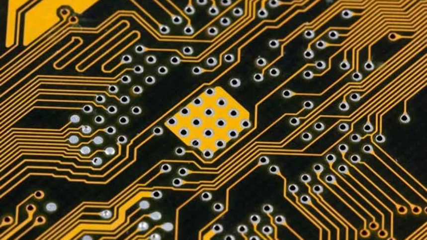
PCB routing is one of the most widely used depanelization methods in PCB manufacturing, especially for designs with complex outlines or strict edge requirements.
Following proper pcb routing guidelines is essential to ensure dimensional accuracy, clean board edges, and stable product quality. As PCB designs become more compact and mechanically sensitive, routing quality has a direct impact on assembly reliability and final product performance.
What Is PCB Routing in PCB Manufacturing?
PCB routing is a depanelization process that uses CNC milling tools to separate individual boards from a production panel.
Unlike V-score depanelization, routing physically removes material along the board outline, allowing greater design flexibility. PCB routing is commonly applied during the final stage of PCB fabrication or after assembly, depending on project requirements.

When PCB Routing Is the Preferred Depanelization Method?
PCB routing is recommended in the following situations:
-
Irregular or complex board outlines
-
Components or copper traces close to the board edge
-
Thick PCBs or boards requiring higher mechanical strength
-
Designs sensitive to mechanical stress
In these cases, routing provides better edge quality and lower stress compared to V-score separation.
Core PCB Routing Guidelines for Design and Manufacturing
Board Outline and Routing Path Design
Smooth routing paths improve edge quality and reduce tool wear. Sharp internal corners should be avoided or designed with proper radius to match routing tool limitations. Well-defined board outlines help ensure consistent dimensional accuracy.
Routing Tool Size and Dimensional Tolerance
Routing accuracy is influenced by the diameter of the milling tool.
Smaller tools allow tighter tolerances but increase machining time and tool wear.
Designers should balance outline precision with manufacturability when applying pcb routing guidelines.
Copper and Component Clearance from Routed Edges
Adequate clearance between copper features and the routed edge is critical. Insufficient clearance may result in copper exposure, delamination, or electrical reliability issues. Components should also maintain a safe keep-out distance from the routing path to avoid mechanical damage.
Tab Routing and Breakaway Tab Design
When boards are connected by tabs, proper tab placement is essential. Tabs should be positioned to provide panel stability while minimizing stress during depanelization. Mouse bites or perforations should be designed to allow clean separation without damaging the board edge.
Panelization and Tooling Considerations
Proper panel layout supports stable routing performance. Tooling holes, fiducials, and panel margins help ensure accurate alignment during CNC routing. Panel rigidity plays a key role in achieving consistent routing quality.

Common Problems Caused by Improper PCB Routing Design
Ignoring pcb routing guidelines may lead to:
-
Rough or uneven board edges
-
Copper exposure or trace damage
-
Excessive mechanical stress during separation
-
Increased scrap rate and rework
These issues can negatively affect both manufacturing yield and end-product reliability.
PCB Routing vs V-Score: Manufacturing Perspective
From a manufacturing standpoint:
-
PCB routing offers greater design flexibility
-
V-score provides faster and lower-cost depanelization for straight-edge boards
-
Routing introduces less mechanical stress
-
V-score is better suited for simple, rectangular designs
Selecting the correct method depends on board geometry, material thickness, and assembly requirements.
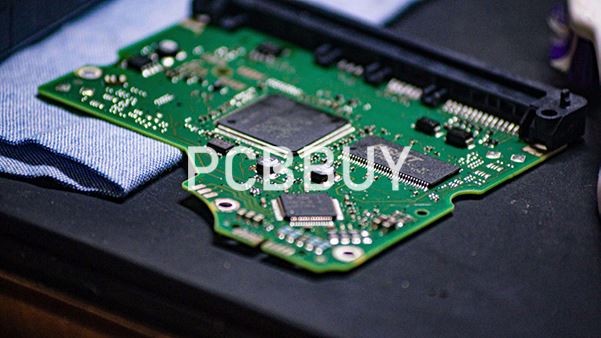
How Manufacturing Capability Supports PCB Routing Accuracy?
CNC Routing Equipment and Process Stability
High-precision CNC routing equipment ensures consistent cutting depth and edge quality.
Controlling spindle speed, feed rate, and tool wear is essential for stable results.
Process Control and Inspection
Dimensional inspection and visual edge checks help verify routing quality.
Consistent monitoring reduces variation between production batches.
Engineering Review and DFM Support
Engineering-led DFM review ensures routing paths, clearances, and tab designs are manufacturable.
Early feedback helps prevent routing-related issues before production begins.
PCBBUY’s PCB Routing Capabilities
PCBBUY supports PCB routing for a wide range of applications, from prototypes to volume production. By combining CNC routing precision with structured DFM review, PCBBUY helps customers achieve reliable depanelization results.
Key capabilities include:
-
Support for complex and irregular board outlines
-
Stable routing quality for export-oriented PCB projects
-
Consistent process control across different production volumes
-
Engineering-driven evaluation of routing feasibility
This approach minimizes manufacturing risk while maintaining high product reliability.
Design Tips to Improve PCB Routing Results
To achieve optimal routing quality, designers should:
-
Maintain sufficient copper and component clearance from board edges
-
Avoid unnecessary sharp corners in outlines
-
Specify depanelization method clearly in fabrication notes
-
Engage the PCB manufacturer early for DFM review
Following these pcb routing guidelines improves both yield and consistency.
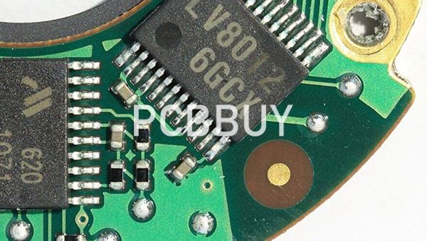
Conclusion
PCB routing plays a critical role in modern PCB manufacturing, particularly for complex and mechanically sensitive designs. By applying established pcb routing guidelines and working with a capable manufacturing partner, routing-related risks can be effectively controlled.
PCBBUY combines engineering expertise and process stability to support reliable PCB routing for global customers.
FAQ
What are PCB routing guidelines?
PCB routing guidelines are design and manufacturing rules that ensure accurate board outlines, clean edges, and reliable depanelization during PCB production.
When should PCB routing be used instead of V-score?
PCB routing is preferred for irregular board shapes, designs with copper near edges, thick boards, or applications sensitive to mechanical stress.
How close can copper be to a routed PCB edge?
Copper features should maintain a safe clearance from the routed edge to prevent exposure or delamination. Exact clearance depends on design and manufacturing capability.
What are breakaway tabs in PCB routing?
Breakaway tabs are small connections that hold boards together during panel processing and allow controlled separation after routing.
Can PCBBUY support complex PCB routing requirements?
Yes. PCBBUY supports complex PCB routing with CNC equipment, DFM review, and stable process control for both prototype and volume production.
Industry Category


