PCB Silkscreen Guidelines
By:PCBBUY 09/06/2021 10:13
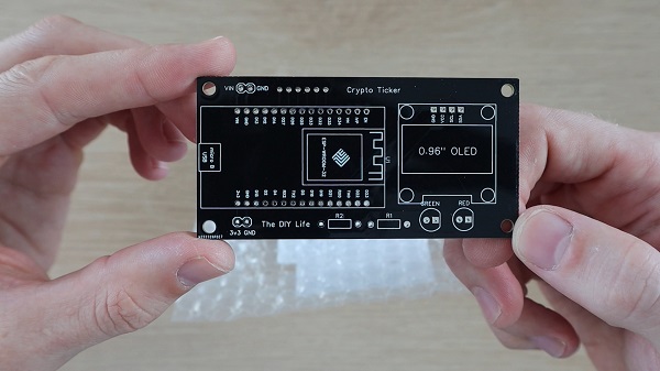
Silkscreen is not only a type of printing process used to apply identification markings on a printed circuit board, but it is also the generic term used to describe the ink markings themselves. This is why the CAD tool layers devoted to these markings are referred to as the silkscreen layers. Printing the silkscreen onto the board is one of the last steps to be completed during printed circuit board fabrication.
If you are going to know the guidelines of PCB silkscreen, welcome to check and read the content below for more professional knowledge about it. Let’s get it!
What is the importance of PCB silkscreen?
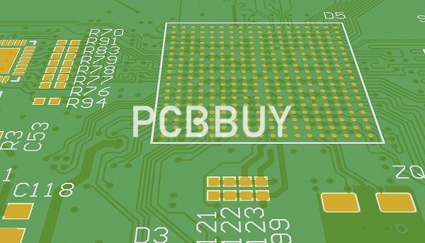
Though the Silkscreen has nothing to do with the functionality of the Printed Circuit Board, the PCB Silkscreen provides information on
· Warning Symbols – The warning symbols indicate the parameters on the high voltage points that you need to avoid or handle.
· Polarity Indicators – It helps you to trace the polarized component’s orientation.
· Locating the parts via reference designators
· It helps in identifying the test points and unique numbers for each board.
· Reference indicators – It helps in identifying the component types via BOM. The Pin 1 indicator helps you to connect the pins to the suitable pads in the footprint. The leading pattern of the component outline would show the placement of a component. The polarity indicators provide you with the polarized component’s orientation
· Pin 1 indicator – It indicates the connection of pins on the correct pads of the footprints.
· Component Online – It enables you to place the components on PCB through indications.
The Component Online wouldn’t be essential for simpler components having a smaller number of pads. However, you would need them for general placement. But you can’t miss out on indicators, Pin 1, Polarity indicators.
What is the process of PCB silkscreen?
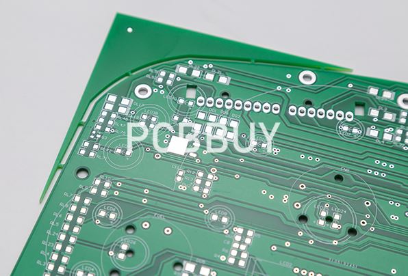
PCB silkscreen is a sub-process in the board tree of solder masking and baking, UV exposure, and development. However, due to its overall impact on the product’s grading and reliability, you can consider it the most sophisticated one among the four in its class.
Preparation
Once the CAD blueprint is finalized, it’s time to move towards hardware implementation. You need to perform some steps to finish the product with high quality. The material selected is then picked up for cleaning, followed by tape trolling and board handling. PCB board then gets ready for printing.
At this point, the PCB Designs should be ready and printed (black) on transparent paper. The designs are placed on the dried silkscreen. In this case, the silkscreen PCB Design should be placed on the prepared silk fabric the way you would like the writings or the markings to appear on the PCB.
Ensuring that the PCB Design paper does not move from where you have positioned it is essential. This can be done by fixing the designs firmly on the surface using TRANSPARENT tape. When this is done, the whole setup (silkscreen and the attached designs) is turned upside down such that the methods face downwards. The top side is then covered with dark cardboard.
The UV light is shown below for about 15 minutes when the PCB silkscreen artwork is fully developed. To expose the developed silkscreen template, pressurized water is used to wash away the emulsion parts that were not exposed to the UV (not cured).
What are the applications of PCB silkscreen?
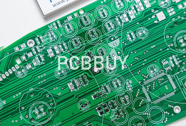
The silkscreen’s primary purpose is to mark the position of the components on the board with an outline, and the part’s unique reference designator. Silkscreen is also used for component polarity and pin 1 indicators. As the component density on printed circuit boards continues to increase, however, there is less space for silkscreen information to be printed. It is common therefore to see reference designators abbreviated as a sequence of numbers, and often the outlines themselves are completely omitted.
This doesn’t lessen the need for component identification though, as these are still important for prototype, NPI, and limited-run boards that will require manual assembly. Component identification is also important for boards that are assembled using automated systems for test and debug purposes, as well as automated optical inspection (AOI), and manual inspection.
Silkscreen markings are also used for marking non-component information as well. This can include the name, part number, and revision of the circuit board, as well as corporate contact information, copyrights, and manufacturing markings. The silkscreen conveys a lot of information about the circuit board, but it isn’t the only method of communicating board information. PCB design CAD systems have many layers built into them that can be used for board information other than the silkscreen, and we will take a look at that next.
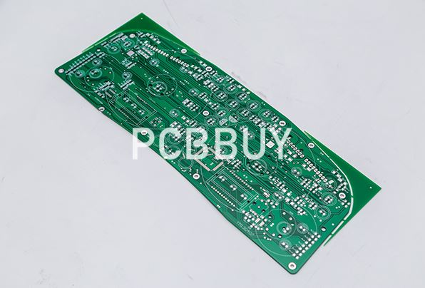
What are the methods of PCB silkscreen?
In the past few years, the primary method of silkscreen referred to using a stencil to directly apply ink to the board surface. Nowadays, there are the two most common silkscreen PCB printing techniques, such as liquid photo imaging (LPI) and direct legend printing (DLP).
Liquid photo imaging (LPI):
This method is used when the line widths are greater than 4 mil. Liquid Photo Imaging is quite similar to the process used for the application of solder mask. In this a liquid photo-imageable epoxy is coated on to the laminate and then exposed with UV light. After this the board is developed and cured. It is much more accurate than manual screening.
Direct legend printing (DLP):
DLP is the most accurate of all these processes but is more expensive. In this process an inkjet projector is used with acrylic ink that is applied onto the raw PCB directly from the CAD data. The ink is cured with UV light as it is printed. It should be noted though that the acrylic ink does not cure on boards with silver finishes.
Industry Category


