
PCB Solder Mask Peel Strength Testing Methods
By:PCBBUY 07/30/2026 15:01
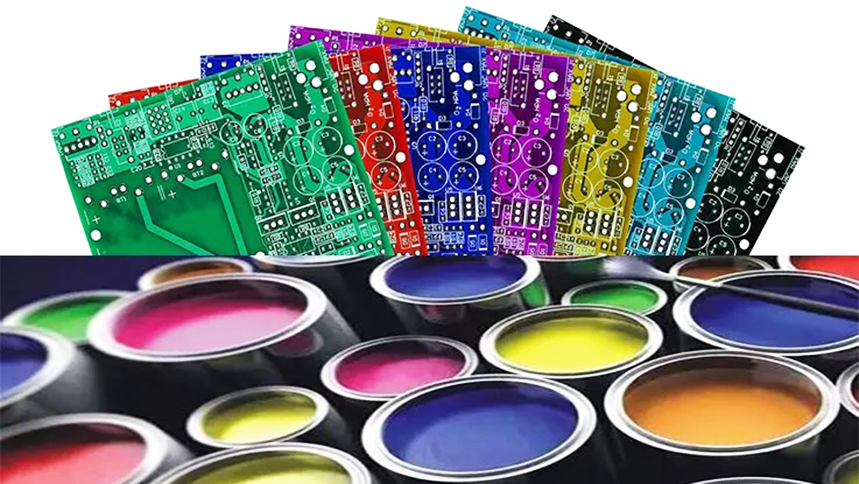
The solder mask is one of the most important protective layers on a printed circuit board. It covers exposed copper areas, prevents solder bridging, protects circuits from environmental contamination, and improves PCB long-term reliability.
However, during PCB assembly and operation, solder mask layers experience various stresses, including:
Thermal cycling during reflow soldering
Mechanical stress during handling
Chemical exposure during cleaning processes
Moisture and environmental aging
If the solder mask adhesion is insufficient, problems such as solder mask peeling, copper exposure, contamination, and electrical failures may occur.
Therefore, PCB solder mask peel strength testing methods are essential quality evaluation procedures used to verify the bonding strength between solder mask materials and PCB surfaces.
As a professional PCB manufacturer, PCBBUY applies strict solder mask process control, advanced surface treatment technologies, and reliability testing methods to ensure durable PCB performance from prototype production to high-volume manufacturing.
What Is PCB Solder Mask Peel Strength?
PCB solder mask peel strength refers to the adhesion force required to separate the solder mask coating from the PCB surface.
It indicates how effectively the solder mask bonds with:
Copper traces
PCB laminate materials
Surface-treated areas
A strong solder mask adhesion layer helps prevent:
Coating peeling
Edge lifting
Copper corrosion
Solder contamination
Assembly failures
Why Solder Mask Adhesion Is Critical for PCB Reliability?
The solder mask serves multiple functions beyond protecting copper
.
Solder Mask Function | Reliability Benefit |
Copper Protection | Prevents oxidation and corrosion |
Electrical Insulation | Reduces short-circuit risks |
Solder Control | Prevents solder bridging |
Mechanical Protection | Improves PCB durability |
Surface Protection | Enhances environmental resistance |
Poor solder mask adhesion can significantly reduce PCB reliability, especially in demanding applications such as:
Automotive electronics
Industrial control systems
Medical devices
Communication equipment
High-temperature electronics
Common Causes of Poor Solder Mask Peel Strength
Solder mask adhesion depends on both PCB manufacturing processes and material characteristics.
Cause | Description | Possible Result |
Poor Surface Cleaning | Residues remain before coating | Weak adhesion |
Copper Oxidation | Contaminated copper surface | Mask peeling |
Incorrect Curing | Insufficient UV or thermal curing | Reduced bonding strength |
Excessive Surface Roughness | Uneven interface | Coating defects |
Material Compatibility Issues | Poor ink selection | Adhesion failure |
Improper Handling | Fingerprints or contamination | Local peeling |
PCB Solder Mask Peel Strength Testing Methods
Different testing approaches are used to evaluate solder mask adhesion and reliability.
1. Tape Adhesion Test (Cross Hatch Test)
The tape adhesion test is one of the most common methods for evaluating solder mask bonding quality.
Testing Process:
Create a cross-cut pattern on the solder mask surface.
Apply standardized adhesive tape.
Remove the tape at a controlled angle.
Evaluate coating removal.
Test Item | Evaluation Purpose |
Coating Removal Area | Measures adhesion quality |
Edge Lifting | Detects weak bonding |
Surface Damage | Evaluates coating durability |
Advantages
Simple operation
Fast inspection
Suitable for production monitoring
Limitations
Mainly qualitative
Limited quantitative data
2. Peel Force Testing
Peel force testing directly measures the force required to remove solder mask material from the PCB surface.
Parameter | Purpose |
Peel Force | Measures adhesion strength |
Peel Angle | Ensures testing consistency |
Peel Speed | Controls test accuracy |
Failure Mode | Identifies bonding problems |
This method provides more quantitative data compared with tape testing.
3. Cross-Section Analysis
Microsection analysis provides detailed observation of the solder mask interface.
It can identify:
Solder mask thickness
Interface bonding condition
Copper surface condition
Internal voids
Coating defects
Inspection Area | What It Reveals |
Copper-Solder Mask Interface | Adhesion quality |
Coating Thickness | Process consistency |
Edge Area | Peeling risk |
Via Coverage | Protection reliability |
PCBBUY uses advanced inspection methods including microsection analysis to verify PCB internal and surface quality.
4. Thermal Stress Testing
During PCB assembly, solder masks experience repeated high temperatures.
Thermal stress testing evaluates whether solder mask adhesion remains stable after heating cycles.
Test Condition | Purpose |
Reflow Simulation | Evaluates assembly durability |
Thermal Cycling | Tests long-term reliability |
Heat Aging | Evaluates material stability |
A high-quality solder mask should maintain strong adhesion after thermal exposure.
5. Chemical Resistance Testing
PCBs may contact:
Flux residues
Cleaning agents
Industrial chemicals
Chemical resistance testing evaluates whether solder mask adhesion remains stable.
Chemical Exposure | Potential Risk |
Cleaning Solution | Surface degradation |
Flux Chemicals | Adhesion reduction |
Industrial Fluids | Coating damage |
Factors Affecting PCB Solder Mask Peel Strength
1. Surface Preparation
Proper copper surface preparation is critical before applying solder mask.
Important processes include:
Cleaning
Micro-etching
Oxide removal
Surface activation
A clean copper surface improves mechanical bonding.
2. Solder Mask Material Selection
Different applications require different solder mask properties.
Solder Mask Type | Characteristics |
Liquid Photoimageable (LPI) Ink | High precision and fine-line capability |
High-Temperature Solder Mask | Improved thermal resistance |
Flexible Solder Mask | Suitable for flexible PCB applications |
Matte Solder Mask | Reduces reflection for optical applications |
PCBBUY supports customized solder mask colors and materials, including standard green, black, white, and special colors.
3. Curing Process Control
Proper curing ensures the solder mask achieves maximum adhesion strength.
Key parameters include:
Process Parameter | Impact |
UV Exposure Energy | Determines pattern accuracy |
Thermal Curing Temperature | Affects hardness and bonding |
Curing Time | Influences mechanical strength |
Solder Mask Thickness Control
Solder mask thickness affects both protection and assembly performance.
Thickness Condition | Potential Issue |
Too Thin | Reduced protection capability |
Too Thick | Component placement problems |
Uneven Thickness | Reliability inconsistency |
Controlled solder mask application helps achieve stable PCB performance.
PCB Solder Mask Quality Control Process at PCBBUY
PCBBUY implements multiple quality control procedures throughout the solder mask manufacturing process.
Incoming Material Inspection
Solder mask ink verification
Material certification review
Storage condition control
Manufacturing Process Control
Surface cleaning monitoring
Precision solder mask printing
UV exposure control
Thermal curing optimization
Final Inspection
Inspection Method | Purpose |
AOI Inspection | Detects solder mask pattern defects |
Visual Inspection | Checks appearance quality |
Thickness Measurement | Confirms coating consistency |
Adhesion Testing | Verifies peel strength |
Electrical Testing | Ensures PCB functionality |
PCBBUY Manufacturing Capabilities for Reliable Solder Mask Performance
For customers requiring high-reliability PCB solutions, PCBBUY provides:
Capability | Customer Benefit |
High Precision PCB Manufacturing | Stable solder mask registration |
HDI PCB Technology | Supports fine-pitch designs |
Multilayer PCB Production | Handles complex structures |
Advanced Surface Finishes | Improves assembly reliability |
AOI and Reliability Testing | Reduces manufacturing risks |
Customized Solder Mask Options | Meets different application needs |
PCBBUY supports PCB production from quick-turn prototypes to volume manufacturing with strict process control.
Best Practices to Improve PCB Solder Mask Adhesion
Recommendation | Benefit |
Maintain Clean Copper Surfaces | Improves bonding |
Select Suitable Solder Mask Materials | Enhances reliability |
Control Curing Parameters | Maximizes adhesion |
Avoid Excessive Handling | Prevents contamination |
Perform Adhesion Testing | Detects process issues early |
Conclusion
Reliable solder mask adhesion is essential for PCB durability, electrical insulation, and long-term performance.
Through effective PCB solder mask peel strength testing methods, manufacturers can evaluate coating adhesion, identify potential defects, and optimize production processes.
By controlling surface preparation, solder mask materials, curing parameters, and inspection procedures, PCBBUY delivers reliable PCB solutions with excellent solder mask performance for demanding electronic applications.
FAQ
1. What is PCB solder mask peel strength testing?
PCB solder mask peel strength testing evaluates how strongly the solder mask coating adheres to the PCB surface and determines its resistance to peeling or separation.
2. Why is solder mask adhesion important?
Strong solder mask adhesion prevents:
Copper exposure
Oxidation
Electrical failures
Coating damage during assembly
3. What are the common PCB solder mask peel strength testing methods?
Common methods include:
Tape adhesion test
Peel force measurement
Cross-section analysis
Thermal stress testing
Chemical resistance testing
4. What causes solder mask peeling on PCBs?
Common causes include:
Poor surface preparation
Copper contamination
Incorrect curing
Material incompatibility
Excessive thermal stress
5. How does curing affect solder mask adhesion?
Proper UV and thermal curing allow solder mask materials to fully bond with the PCB surface. Insufficient curing can result in weak adhesion and peeling.
6. Can solder mask peel strength affect PCB assembly?
Yes. Poor solder mask adhesion may cause solder contamination, reduced insulation performance, and reliability issues during PCB assembly.
7. How does PCBBUY ensure solder mask reliability?
PCBBUY controls solder mask printing, curing processes, surface preparation, AOI inspection, adhesion verification, and final electrical testing to ensure consistent PCB quality.
Industry Category








