PCB Stackup Guidelines to Building Reliable and High-Performance Boards
By:PCBBUY 10/31/2025 17:25

Designing a Printed Circuit Board is not only about schematic connections and routing techniques. One of the most influential factors affecting signal integrity, mechanical strength, thermal behavior, and overall electronic performance is the PCB stackup. Understanding proper PCB stackup guidelines is essential for engineers who aim to build stable, low-noise, and production-ready boards.
At PCBBUY, we support customers from prototype development to full-scale manufacturing, providing engineering consulting, stackup recommendations, and controlled impedance validation. The goal is simple: help you build a PCB that performs reliably—both in testing and in real-world applications.
1. What Are PCB Stackup Guidelines and Why Do They Matter?
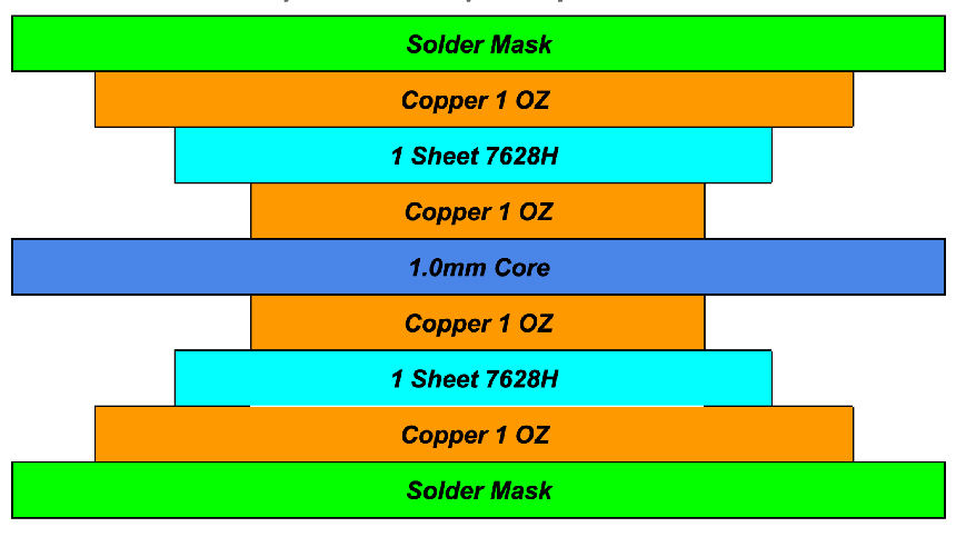
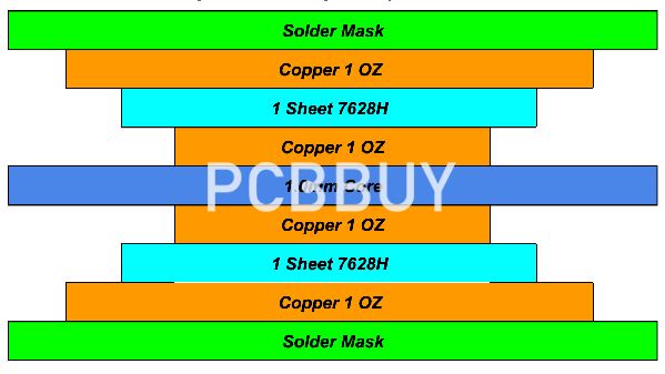
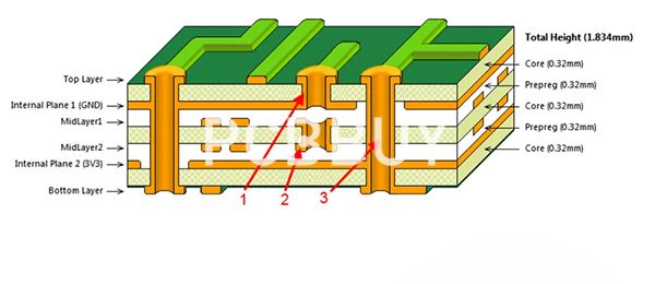
A PCB stackup is the arrangement of copper layers and insulating dielectric layers within the board. The way these layers are structured directly affects:
-
Signal transmission quality
-
Electromagnetic interference (EMI) behavior
-
Mechanical durability
-
Heat distribution and dissipation
-
Cost and manufacturability
When stackup planning is correct, routing becomes easier, impedance remains stable, and product reliability increases. When planned poorly, even the best schematic design may fail during testing or high-speed operation.

2. Essential Material Considerations in PCB Stackup Guidelines
The PCB stackup is determined by the selection of materials and layer thicknesses. Important factors include:
|
Parameter |
Impact |
|
Core & Prepreg |
Defines board rigidity and final thickness |
|
Copper Weight |
Influences current carrying capacity & heat dissipation |
|
Dielectric Constant (Dk) |
Affects signal propagation, especially high-speed |
|
Dielectric Thickness |
Necessary for controlled impedance matching |
At PCBBUY, we offer flexible material options such as FR4, High-Tg FR4, Rogers, Polyimide, and Hybrid laminates. Engineers receive stackup recommendations based on signal speed, operational environment, and product requirements—not generic templates.
3. Common PCB Stackup Guidelines for Layer Configuration
Different applications require different stackup styles:
2-Layer PCB Stackup
Used in cost-sensitive consumer devices, LED drivers, power supplies.
4-Layer PCB Stackup
Ideal for IoT modules and compact boards needing reduced noise.
Typical structure:
Signal / Ground / Power / Signal
6-Layer and 8-Layer PCB Stackup
Required for industrial control systems, FPGA boards, and automotive modules, where signal integrity is critical.
HDI (High-Density Interconnect) Stackup
For high-speed SoC, 5G modules, and wearables, using:
-
Blind / Buried vias
-
Microvias
-
Sequential lamination
PCBBUY supports HDI from Type I to Type III, meeting the needs of compact, fine-pitch device designs.

4. PCB Stackup Guidelines for High-Speed Signal Integrity
High-speed digital and RF circuits require special stackup considerations:
-
Controlled impedance (50Ω / 90Ω differential pairs)
-
Minimizing crosstalk through solid reference planes
-
Isolating high-frequency layers away from switching power regions
-
Using low-Dk materials for RF routing
PCBBUY provides impedance simulation and cross-section testing, ensuring production results match design expectations.
5. How PCB Stackup Influences Cost
|
Factor Affecting Cost |
Explanation |
|
Layer Count |
More layers → higher material and lamination cost |
|
Material Type |
Rogers, Polyimide, and High-Tg cost more than FR4 |
|
HDI Features |
Microvias and sequential lamination increase processing steps |
|
Copper Thickness |
Heavy copper requires deeper etching and plating control |
PCBBUY works with customers to balance budget vs. performance, helping avoid unnecessary complexity that does not improve end-use reliability.
6. PCBBUY’s Engineering Strength in PCB Stackup Design
What differentiates PCBBUY is not just manufacturing, but engineering:
-
Dedicated DFM and stackup consulting before production
-
Controlled impedance tolerance ±10%
-
Automated lamination and precise copper distribution management
-
Full cross-section inspection for quality verification
-
Support for Prototype → Small Batch → Mass Production
Whether you’re building a medical device, an automotive controller, or a telecommunications module, PCBBUY ensures the stackup is aligned with industry reliability requirements.

7. Case Study: Optimized 8-Layer Stackup for a Compact Wearable Device
Challenge: High-speed BLE + MCU + Power Management in limited space
Approach:
-
Reduced EMI by adding a continuous ground reference plane
-
Balanced power distribution via dedicated power plane
-
Used low-loss dielectric to maintain RF clarity
Result:
Signal noise decreased measurably, power stability improved, and device passed EMC tests on first submission.
Conclusion:
A thoughtfully designed stackup isn’t just an engineering preference—it is the core reason why a PCB performs well under stress, high-speed transmission, and long-term operation.
PCBBUY provides experienced stackup consulting, robust manufacturing capabilities, and strict quality control to ensure your board performs exactly as intended.
FAQ — PCB Stackup Guidelines
Q1: How do I know how many layers my PCB needs?
It depends on signal complexity, EMI requirements, and board size. PCBBUY engineers can evaluate and recommend a suitable layer count.
Q2: Why is controlled impedance important in stackup design?
It ensures reliable signal transmission, especially for high-speed or RF circuits.
Q3: Can PCBBUY support HDI multilayer stackups?
Yes. PCBBUY supports microvias, blind/buried vias, and sequential lamination for complex HDI boards.
Industry Category


