
PCB Surface Finish Selection for Fine-Pitch BGA: How Should Engineers Choose?
By:PCBBUY 09/30/2026 15:45
As BGA packages become smaller and their ball pitch decreases, PCB surface finish selection becomes increasingly important. The surface finish is not simply a protective coating for exposed copper. For fine-pitch BGA assembly, it directly affects pad planarity, solderability, process consistency, and the manufacturing margin available to the assembly process.
Therefore, PCB surface finish selection for fine-pitch BGA should be based on the complete assembly requirement rather than on cost or the surface appearance of the finished board alone.
ENIG, ENEPIG, OSP, HASL, immersion gold, and other finishes each have different characteristics. The appropriate choice depends on BGA pitch, assembly process, storage conditions, reliability requirements, and whether the PCB contains other special features such as connectors or wire-bonding areas.

Why Does Surface Finish Matter for Fine-Pitch BGA?
BGA solder joints are located underneath the component package, which makes them fundamentally different from easily visible leads on conventional components.
As BGA pitch becomes finer, the available pad area and spacing become smaller. Variations in pad height or surface condition can therefore consume part of the assembly process margin.
A suitable surface finish should provide:
-
A sufficiently planar pad surface
-
Consistent solderability across the BGA footprint
-
Good protection against copper oxidation before assembly
-
Stable performance during the specified reflow process
-
Compatibility with the customer's storage and handling conditions
-
Appropriate reliability for the final application
It is also important to distinguish surface finish selection from solder paste and reflow-profile optimization. A good surface finish cannot compensate for poor stencil design, inaccurate paste printing, incorrect component placement, or an unsuitable reflow profile.
ENIG for Fine-Pitch BGA
ENIG, or Electroless Nickel Immersion Gold, is widely used for fine-pitch SMT and BGA applications because it provides a relatively flat surface compared with solder-levelled finishes.
The nickel layer acts as a barrier over the copper, while the immersion gold protects the surface and provides a suitable solderable interface.
For fine-pitch BGA, the main advantages of ENIG include:
-
Good pad planarity
-
Consistent surface appearance and geometry
-
Good solderability when properly processed
-
Compatibility with dense SMT layouts
-
No additional solder coating that creates a pronounced pad profile
However, ENIG requires controlled chemical processing. Nickel surface condition and gold deposition must be properly controlled because surface-finish defects can directly affect solder-joint quality.
For applications such as automotive electronics, industrial control, power electronics, energy-storage equipment, and embodied robotics, ENIG can be considered when the PCB requires a flat surface for dense SMT/BGA assembly and the overall assembly process is compatible with the finish.

When Is ENEPIG Worth Considering?
ENEPIG adds a palladium layer between electroless nickel and immersion gold.
Its main value is not simply that it is another “gold finish.” Rather, the additional palladium layer changes the metallurgical structure of the surface and can make ENEPIG attractive when the PCB has requirements beyond conventional soldering.
For example, ENEPIG may be considered when a design combines fine-pitch SMT with specific wire-bonding requirements or when the customer's reliability requirements justify the additional process complexity and cost.
For a PCB containing only conventional BGA solder joints, engineers should not automatically select ENEPIG simply because it is a more complex finish. The surface finish should be matched to the actual assembly and product requirements.
What About OSP and HASL?
OSP provides a thin organic protective layer over exposed copper and has the advantage of maintaining a very flat copper surface. This makes it technically relevant to fine-pitch applications.
However, OSP is more dependent on storage, handling, and assembly conditions. The manufacturing and assembly schedule should therefore be considered before selecting it for a BGA-heavy product.
HASL, including lead-free HASL, provides good solderability but produces a solder-coated pad surface that is less planar than finishes such as ENIG or OSP.
For dense fine-pitch BGA footprints, pad planarity becomes increasingly important. Therefore, HASL should be evaluated carefully rather than selected simply because it has a lower fabrication cost.
Surface Finish Selection for Fine-Pitch BGA
|
Surface finish |
Main characteristic |
Fine-pitch BGA consideration |
Typical engineering consideration |
|
ENIG |
Flat nickel/gold surface |
Well suited to dense SMT and BGA structures |
Balance planarity, solderability, storage and process control |
|
ENEPIG |
Nickel/palladium/gold structure |
Suitable when additional surface-function requirements exist |
Consider wire bonding, reliability requirements and cost |
|
OSP |
Thin organic protective layer |
Flat surface can support fine-pitch assembly |
Pay close attention to storage, handling and assembly timing |
|
HASL |
Solder-coated surface |
Less suitable when very high pad planarity is required |
More appropriate when fine-pitch constraints are limited |
|
Immersion gold / other applicable finishes |
Depends on specific process structure |
Evaluate according to pad function and assembly requirements |
Confirm compatibility with soldering and any special pad functions |
The table is a design-selection framework rather than a universal ranking. The actual finish should be confirmed against the customer's assembly process and fabrication specification.
Fine-Pitch BGA Requires More Than the Right Surface Finish
Surface finish is only one part of BGA manufacturing control.
For a fine-pitch BGA, engineers should also consider pad geometry, solder mask registration, layer registration, via placement, board warpage, and the relationship between the PCB design and the assembly stencil.
This becomes particularly important when HDI structures are used to escape dense BGA packages.
For example, a fine-pitch BGA may require laser blind vias to create additional routing channels. In this situation, the PCB manufacturer must control not only the surface finish but also the underlying HDI structure and registration between layers.
A theoretically suitable surface finish cannot solve an insufficient routing or registration margin.
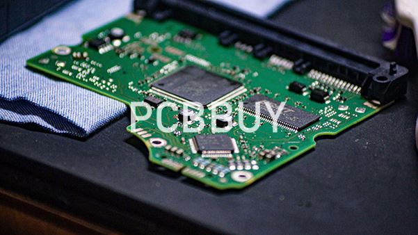
How PCBBUY Supports Fine-Pitch BGA PCB Manufacturing
For advanced BGA PCB designs, PCBBUY combines surface-finish options with HDI and precision manufacturing capabilities rather than treating surface treatment as an isolated process.
PCBBUY supports ENEPIG, ENIG, OSP, HASL, immersion gold, immersion tin, and selective electroplated gold. This allows the surface finish to be selected according to the function of each PCB area and the customer's assembly requirements.
For high-density BGA routing, PCBBUY supports first-order and second-order HDI, with a minimum laser blind-via diameter of Φ0.075 mm and a minimum mechanical blind-via diameter of Φ0.15 mm.
These figures represent manufacturing capabilities, not recommended BGA design dimensions for every project. Actual via geometry should be reviewed against the BGA pad size, dielectric thickness, stackup, registration requirements, and reliability objectives.
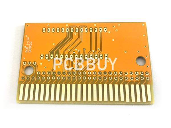
PCBBUY also supports selective electroplated gold from 3–100 µin and gold fingers up to 100 µin, allowing different surface treatments to be considered for different functional areas of the same PCB when the design requires it.
For multilayer designs using different material systems, asymmetric and heterogeneous mixed-material lamination is also supported. This can be relevant when a BGA board combines dense digital routing with sections requiring different electrical, thermal, or material characteristics.
Surface Finish and Quality Control
Fine-pitch BGA manufacturing requires process control from copper pattern formation through surface finishing and final inspection.
A manufacturer's inspection capability should therefore be considered alongside its surface-finish menu.
PCBBUY supports AOI, flying-probe testing, and four-wire low-resistance testing. These methods address different aspects of PCB quality and electrical verification.
For example, AOI can be used to inspect relevant PCB pattern and surface-related features, while flying-probe and four-wire low-resistance testing provide electrical verification appropriate to the product's requirements.
The exact inspection plan should be established according to the PCB design, customer specification, production volume, and required acceptance criteria rather than assuming that one inspection method is sufficient for every BGA board.
How Should Engineers Select the Finish Before PCB Fabrication?
Before releasing a fine-pitch BGA design for production, engineers should review several questions:
What is the BGA pitch and pad geometry?
The finer the geometry, the more important pad planarity and process consistency become.
How soon will the PCB be assembled after fabrication?
This is particularly relevant when considering finishes whose storage and handling window is more process-sensitive.
How many thermal cycles will the board experience?
The complete assembly and rework process should be considered rather than evaluating the first reflow cycle alone.
Are there wire-bonding or special-contact requirements?
If so, the surface finish may need to satisfy requirements beyond ordinary BGA soldering.
Does the PCB contain both BGA areas and other functional surfaces?
Different areas may require different surface-treatment approaches, depending on their function and customer requirements.
What reliability and shipment conditions apply?
For automotive, industrial control, power, energy storage, new-energy, and embodied-robotics applications, the finish should be selected together with the product's assembly and service requirements.

Conclusion
PCB surface finish selection for fine-pitch BGA should be treated as part of the overall PCB manufacturing and assembly strategy, not as a simple material-cost decision.
ENIG is a widely applicable option for dense BGA and SMT structures because of its planar surface and established manufacturing process. ENEPIG may be appropriate when additional surface-function requirements justify its more complex structure. OSP can provide a flat surface but requires appropriate control of storage, handling, and assembly conditions. HASL remains useful for many conventional PCB applications but requires greater consideration when very fine-pitch BGA pad planarity is critical.
For advanced BGA boards, surface finish should ultimately be evaluated together with HDI structure, registration, pad geometry, material selection, inspection, and the customer's assembly process.
With ENIG, ENEPIG, OSP, HASL, immersion finishes, selective gold, first- and second-order HDI, Φ0.075 mm minimum laser blind vias, mixed-material lamination, and AOI, flying-probe, and four-wire low-resistance testing, PCBBUY can provide manufacturing support for demanding PCB applications across automotive, industrial control, power and electrical systems, power supply, energy storage, new energy, and embodied robotics.
FAQ
1. What surface finish is commonly considered for fine-pitch BGA PCBs?
ENIG is commonly considered because it provides a relatively planar surface and is widely used for dense SMT and BGA assembly. However, the final choice should depend on the complete assembly and reliability requirements.
2. Is HASL suitable for fine-pitch BGA?
HASL provides good solderability, but its surface is less planar than finishes such as ENIG and OSP. When BGA pitch and pad geometry make coplanarity particularly important, engineers should evaluate other finishes.
3. Is OSP suitable for BGA assembly?
OSP can be used for fine-pitch and BGA applications because it provides a flat surface. However, storage, handling, assembly timing, and the number of thermal cycles should be carefully considered.
4. When should ENEPIG be considered instead of ENIG?
ENEPIG may be considered when the PCB has additional requirements such as specific wire-bonding functions or other surface-related requirements that justify the additional palladium layer and process cost.
5. What HDI capability does PCBBUY provide for dense BGA routing?
PCBBUY supports first-order and second-order HDI, with a minimum laser blind-via diameter of Φ0.075 mm and a minimum mechanical blind-via diameter of Φ0.15 mm. The final via dimensions should be determined through engineering review of the actual stackup and BGA layout.
6. Can different surface finishes be used for different PCB areas?
Yes, depending on the PCB design and manufacturing process. For example, solderable areas and functional contact areas may have different surface requirements. The appropriate finish structure and process should be confirmed during engineering review.
7. Which applications are relevant to PCBBUY's BGA and advanced PCB capabilities?
PCBBUY's capabilities are applicable to PCB projects in automotive, industrial control, power and electrical systems, power supply, energy storage, new energy, and embodied robotics, where dense interconnection, controlled surface finishing, and manufacturing consistency can be important.
Industry Category








