PCB Via Current Calculator
By:PCBBUY 08/25/2021 09:16

Trace and via current-carrying capacity are legitimate design points to focus on when designing a new board that will carry high current. The goal is to keep conductor temperatures below some appropriate limit, which then helps keep components on the board cool.
In this passage we will focus on everything about PCB via current and if you are curious about it, please check and read the content we prepare below for more professional information.

What are the guidelines of PCB via current?
The following via design guidelines using in PCB design process are recommended to enhance the engineering performance, saving cost, increasing the stability of the products.
Vias in high speed circuit design
1. Avoid using vias and layer changes if possible to avoid signal distortion.
2. Do not use via in high frequency clock transmission line.
3. When possible, remove any unnecessary pads on vias because these pads create parallel plate capacitance.
4. Smaller vias have lower capacitance. Short length, larger diameter vias have lower inductance. Both parasitic elements can have detrimental affects, but it is often the parasitic inductance element that provides an unexpected series impedance that creates signal transmission problems.
5. Keep the number of vias of the two differential traces the same to minimize the skew and phase difference.

What is the importance of PCB via current calculator?
All vias have inductance and resistance. Therefore, if you are routing a trace from one side of the PCB to the other and need low inductance or resistance, use multiple vias. However, you must also take the size of the via into consideration. As I am sure you remember, resistivity and conductivity are inversely related. So, the size of a via is especially crucial since they have resistance values. In general, larger vias have lower resistance. That is why larger vias are especially useful in grounding filter capacitors and high current nodes.
Having addressed the inductance and resistance properties of vias, it stands to reason that they can affect actual current flow. Like wires, resistance in vias produce a loss of energy, and it is usually in the form of heat. This side-effect is detrimental to PCB functionality. Therefore, being able to calculate the current carrying capacity of vias is a necessity of proper PCB design.
Although there are complex variables involved in these calculations, all is not lost. With accuracy being today’s go-to buzz word when considering PCB design, it is no surprise that the calculations we need to complete these designs are very crucial. In terms of via current forecasts, there is one standard that receives universal acceptance; IPC–2152.
What are the applications of PCB via current?
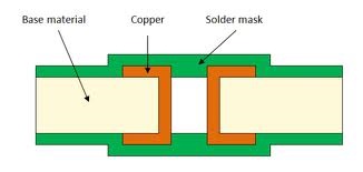
As I am sure you know, the primary purpose of any (PCB quote) via is to provide a path for passing an electrical signal from one circuit layer to another utilizing a plated hole wall. Although via are also used to dissipate heat as well in some applications.
So, if there is an electrical signal, then there is current. The via’s ability to conduct these electrical signals (current) is the difference between a PCB functioning properly or not at all. When a via is unable to conduct current properly, this is when you have mishaps such as short circuits or even total electrical circuit failure occur.
Therefore, it stands to reason that one must be able to measure this current as well. Also, the task of calculating via current by today’s PCB designers is usually with a via current calculator.

What is the capacity of PCB via current?
For whatever number that gives you, compare the closest smaller trace width.
Via cross section, the related questions to all of you PCB fabrication gurus out there are:
Since vias are not created in the same way as the trace plating is, can that simple formula be used? While the trace copper is laminated onto a nice smooth PCB surface, the vias are typically created by deposition of copper dust in the via and then electroplating more copper. Then the surface finish is applied to all of the exposed metal. The via walls would generally be rougher than the flat substrate surface.
Further, since airflow will be somewhat restricted in a via relative to a surface, should the via effective width be compared to an internal trace instead of an exposed surface trace? Should it be a compromise between the two?
Via current calculations are an integral part of overall PCB design or at least it needs to be. The fact remains that the complexity of PCB’s continues to increase, and with it, the number of components which leads to the need for multiple layers.
Vias are a necessity in designs because they can afford the designer with shorter paths without sacrificing performance or signal integrity. Therefore, the need for accuracy and efficiency is paramount when calculating via currents as to avoid PCB failures or degradation in overall PCB performance.
Industry Category


