PCB assembly inspection checklist
By:PCBBUY 07/29/2021 09:20

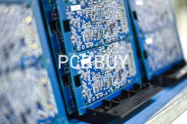
As the essential technology during PCB manufacturing process, PCB assembly will affect the quality and performance of the finished products. It’s increasingly more significant to set inspection and test procedures and pick up inspection technologies during SMT assembly. In this passage, we will introduce you PCB assembly inspections and tests. Please check and read the content we prepare for more information.
What are the inspections of PCB assembly?
During the process of SMT assembly, leading inspections and tests that are usually used include visual inspection, AOI (Automated Optical Inspection), X-ray inspection and ICT (In-circuit Test).
Visual Inspection
As far as its literal meaning goes, visual inspection refers to the inspection during which staff determine whether product quality conforms to manufacturing standard directly by observing target product with the help of naked eyes. Visual inspection has been widely applied due to its handy operation and low cost while its implementation is closely related with staff’s experience and work attitude. Plus, it fails to be used in the inspections on 0603 or 0402 packages and some fine-pitch components owing to physical limitations. Along SMT manufacturing line, visual inspections are usually applied after solder paste printing, before reflow soldering and after reflow soldering among which the visual inspection carried out prior to reflow soldering is of the most significance when it comes to SMT assembly quality guarantee.
AOI
Usually used just after post-reflow visual inspection, AOI test is applied to expose defects by the application of high-speed and high-accuracy optical process technology. As AOI machine is working, camera rapidly captures images of inspected targets and will compare them with proper parameters that have been restored in the database so that PCB (Printed Circuit Board) defects will be found out and automatically marked through monitor.
The advantages of AOI equipment include easy-to-learn programming and simple operations. However, AOI fails to be used on structural inspections of components with solder joints that are visionless, BGA (Ball Grid Array) for example. In addition, AOI also fails to display the unobvious defects such as component and PCB warpage.

ICT
Devices for the implementation of ICT include flying probe tester and bed of nails tester and test targets are usually modules going through SMT assembly. Electrical performance of components on PCB can be tested by ICT and the defects include missing parts, wrong parts, defective components, shorts, opens and defective assembly etc.
X-ray Inspection
X-ray inspection is used to inspect solder joint quality through scanning on PCB. Soldering quality can be clearly reflected thanks to the penetration of x rays. Compared with AOI, X-ray inspection is more capable of displaying more dimensions of solder joints but features higher cost.
The inspections introduced above feature their own attributes and they should be appropriately picked up in accordance with the specific targets to be inspected during SMT assembly. The comprehensive application of multiple inspection methods is helpful in reducing rework cost and improving percent of pass.
What are the incoming inspections of PCB assembly?
Incoming inspection is usually implemented by naked eyes, that is, visual inspection, and its inspection targets include PCB bare boards, components and solder paste.

Incoming Inspection on PCB Bare Board
Size and Appearance Inspection
Bare board size inspection items include aspect ratio, space and tolerance, and PCB edge size. Its appearance can be inspected by PCB inspector with inspection targets featuring interior/exterior layers of multi-layer PCB, single/double-sided PCB and inspection items opens, shorts, scrapes, line width, tracing and other defects.
Warpage Inspection
The manual measurement method on PCB warpage is to measure the distance from the fourth corner to table surface while tightly pressing the other corners of the board to table surface.
Solderability Inspection
The focus of SMT solderability inspection lies in pad and electroplated through hole inspection, including edge edge dip test, rotation dip test, wave dip test and solder ball test.
Internal Defect Inspection
Microsection technology is usually applied for PCB internal defect inspection with inspection items covering thickness of copper with tin-lead alloy, alignment between conductive layers, lamination etc.

Incoming Inspection on Components
First, incoming inspections should be made on components in accordance with corresponding standard and regulation. Items concerning components inspection include the following aspects: whether component performance, specification and package conform to order requirement, to product reliability requirement, to assembly technology and assembly equipment requirement, to storage requirement. Apart from the above general inspections, lead coplanarity, lead coating layer thickness should be inspected to ensure they are compatible with technology requirement and capable of standing 10-cycle heating.
Incoming Inspection on Solder Paste
Qualified solder paste should feature metal percent in the range from 85% to 92%, qualified solder joint curing strength, adhesion in the range from 200Pa. s to 800Pa. s etc.
Industry Category


