PCB edge plating guidelines
By:PCBBUY 08/10/2021 17:18

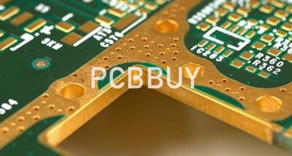
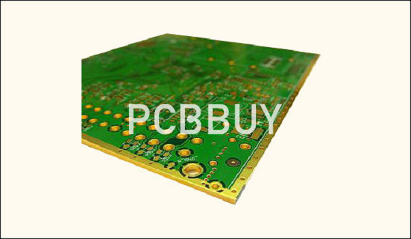
Since plating is very common in PCB manufacturing, sometimes PCB manufacturers can extend this technique to edge plating, connecting the top and bottom planes of a PCB by electroplating around its external edges. In this passage, we will focus on PCB edge plating and please check and read the content we provide.
What are the applications of PCB edge plating?
Several industries require edge-plated boards, especially in applications that require better support for connections such as for boards that slide into metal casings. Edge plating has other uses as well as it improves the current-carrying capabilities of the board, provides edge connection and protection, and offers the possibility of edge soldering to improve fabrication.
Although edge plating on printed circuit boards is a simple addition in most cases, fabricators need specialized equipment and trained personnel for the process. Designers must take care that internal power planes do not come up to the edge, and fabricators must make sure there is a gap before they take up edge plating. Designers must make sure there is a band of copper on both edges of the top and bottom side, as the plating will connect to these copper bands.
Now edge plating PCB has been widely used in many industries, particularly in applications that need better support for connections, for example for circuit boards that slide into metal casings. What’s more, edge plating has other benefits as follows:
· Improve the current-carrying capabilities of PCB;
· Offer edge connection and protection;
· Offer the possibility of edge soldering to improve fabrication.
In fact, PCB manufacturers need to fabricate the circuit boards with specialized equipment and trained personnel for the process although edge plating on printed circuit boards is a simple addition in many cases. In addition, designers need to make sure that there is a band of copper on both edges of the top and bottom side, because the plating will connect to the copper bands.
So we will try our best to do the precise checks so that keep everything safe. For example, the PCB castellation should never lead the internal power planes to the edge of the circuit board, as it can make the edge plating short-circuited. What’s more, we need to make sure that there is a gap before the edge plating process while fabricating the circuit board for edge soldering.

What is the process of PCB edge plating?
As you know, there are a great deal of challenges for a multilayer PCB manufacturer mainly in how to prepare the plated edges and the life span adhesion of the plated material, what’s more, it needs the precision handling in PCB manufacturing that is used for edge PCB soldering. We can make sure that the PCB edge castellation thoroughly prepares edges surfaces, which applies the plated copper for prompt adhesion and processes the circuit board to make sure the long-term adhesion between each layer.
Needless to say, we can control the potential hazard for plated through hole and edge plating with a controlled process during printed circuit board manufacturing for edge soldering. So the most important concern is the creation of burrs, which result in discontinuities in plated through hole walls and limits the life of adhesion of the edge plating.
The outer contours, to be metalized, must be milled before through-hole plating process, as the metallization of the edges take place during this fabrication step. After the deposition of copper, the intended surface finish is finally applied to the edges.
Fabrication Issues:
1. Copper Peeling -Plating over a large substrate surface can lead to the plated copper peeling due to a lack of adhesion strength. We address this by first roughening the surface through a combination of chemical and other proprietary means. Next, we employ direct metallization, which has a higher copper bond strength, to prepare the surface for plating.
2. Burrs -Often edge plating, especially on castellation holes, can result in burrs from the final machining process. We apply a modified, proprietary process flow that results in the burrs being polished down to the edge of the feature.
Fab Note:
1. The antenna position of the gold pad is too large, affecting customer soldering or signal transmission.
2. The inner edge pad is connected to the wires on the board, resulting in a short circuit.
3. The stamp hole is designed at the edging groove and must be handled in the 2nd drilling process.
4. Through the process-related manufacture of the individual PCBs as a panel, a continuous metallization of the outer edges is not possible. No metallization can be applied where the small panel bridges are located.
5. One request, the slide plating metallization can be covered with solder mask.
When purchasing edge plating boards, you must confirm with your PCB supplier the possibility of manufacturing PCBs with plating process, and extent to which the fabricator can edge plate the PCB. Your Gerber files or fab drawing should indicate in a mechanical layer where they need slide plating, and the surface finish they need on it. Most manufacturers prefer a selective ENIG as the only surface finish suitable for round castellation.
What is the limitation of PCB edge plating?
Because fabricators need to hold the circuit boards within the production panel in PCB prototype, they can’t plate the complete-length edge. Therefore, there are some gaps required to place rout tabs. It needs routing the circuit board profile at the place when fabricating the circuit boards with edge plating, and the edge plating is required before starting the process of through-hole plating, which remove v-cut scoring on a PCB that needs to undergo edge plating.
Industry Category


