PCB inspection methods
By:PCBBUY 07/20/2021 09:18

Inspecting PCBs throughout the design, manufacturing and assembly processes is crucial to assuring that your product meets quality standards and operates as expected. Today, PCBs are complex. While this complexity makes room for lots of new capabilities, it also creates more chances for failures. As PCBs have gotten more advanced, so have the inspection techniques and technologies used to ensure their quality.
What is the importance of PCB inspection? What are the methods of PCB inspection? In this passage, we are going to talking about it and please check and read the content below for more information.
If you want to order PCB product, please check and custom your order online.
What is the importance of PCB inspection?
Inspection is a critical step in any PCB production process. It can help you to catch defects so that you can correct them and improve your overall operation.
Inspecting your PCBs can uncover any defects that may have occurred during manufacturing or assembly. It can also help to reveal any design flaws that may exist. Checking PCBs after each phase of the process enables you to catch flaws before moving on to the next stage, which can save you from wasting further time and money on a defective product. It can also help you catch one-off defects that affect one or several PCBs. This process helps to ensure consistent quality among your boards and final products.
Without a proper PCB inspection procedure in place, flawed boards may make it into the hands of customers. If a customer receives a faulty product, your company may lose money through warranty payments or returns. The customer will also lose some of the trust they had in your company, and your reputation will suffer. This situation can result in missed opportunities if that customer takes their business elsewhere.
What are the PCB inspection methods?
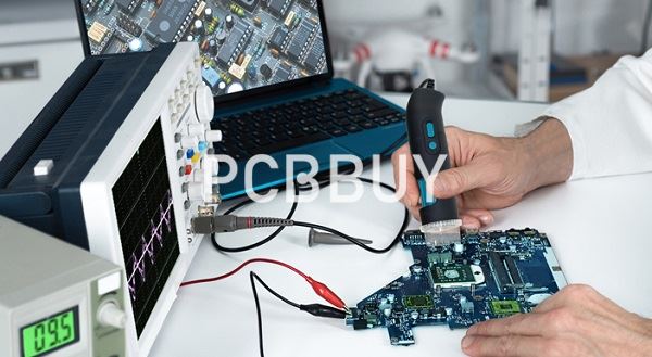
What is PCB inspection? In order to make sure that PCBs are performing as intended, manufacturers must verify all components are assembled correctly. This is done with a range of techniques including simple manual inspections to automated tests that use advanced PCB inspection equipment.
Manual visual inspections are a great starting point. For simpler units, they may be all that’s needed. At Electronic Manufacturing Services Group, we perform a manual visual inspection under magnification of every board we produce to ensure we meet all customer expectations. We also offer other inspection services that involve the use of advanced equipment. This equipment can speed up the inspection process and may be necessary for more complex board types, such as multi-layer boards and those with high numbers of components.
Manual Visual Inspection
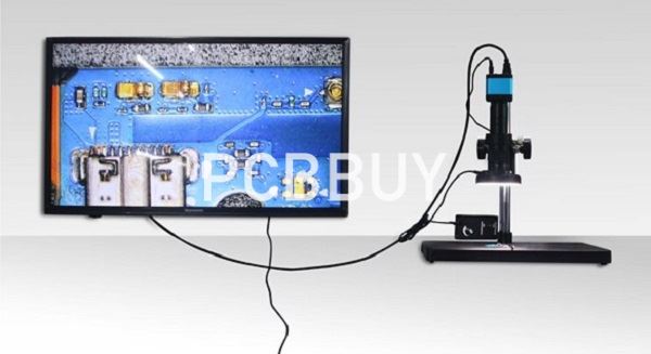
The simplest form of PCB inspection is manual visual inspection (MVI). To perform this type of test, a worker looks over the board either with the naked eye or through magnification. They’ll compare the board to the design documents to ensure that all specifications were met. They’ll also look for common defaults. The type of defects they look for vary depending on the kind of board they’re checking and the components on it.
It can be useful to perform an MVI after nearly every step in the PCB production process, including assembly. EMSG conducts an MVI under magnification of every board we produce. You may also wish to follow MVI with a more advanced, comprehensive examination.
Inspection staff members inspect nearly every aspect of a board and look for various common defects on each of them. A typical visual PCB inspection checklist might include the following:
· Ensure that the board’s thickness is correct, and check for surface roughness and warpage.
· Check the dimensions of the assembly match the specification, and pay particular attention to dimensions related to electric connectors.
· Inspect the integrity and clearness of conductive patterns, and check for solder bridging, open circuits, burrs and voids.
· Check the surface quality, then look for the existence of pits, dents, scratches, pinholes and other defects on printing traces and pads.
· Verify that all vias are in the correct positions. Make sure they aren’t missed or inaccurately punched, that their diameter matches design specifications and that there are no voids or nodules.
· Inspect the firmness, roughness and brightness of pad plating, and check for any bulge defects.
· Assess coating quality. Check the color of plating flux and whether it is even, firm and in the correct position.
Automated Optical Inspection
You can also use a PCB inspection machine to conduct a visual inspection. This method is called automated optical inspection (AOI).
An AOI system conducts an inspection using several light sources and one or more still or video cameras. The light sources light up the board from various angles. The cameras then take still images or video of the board, compiling them to create a complete picture of the unit. The system then compares the images it captures with information about what the board should look like taken from design specifications or an approved completed unit.
Both two-dimensional and three-dimensional AOI equipment is available. 2D AOI machines use colored lighting from multiple angles and side-angle cameras to inspect components for which height is a factor. 3D AOI equipment is newer and can quickly and accurately measure component height.
An AOI can find many of the same defects that an MVI can, including nodules, scratches, open circuits, solder thinning, missing components and more. At EMSG, we sometimes use AOI, especially for more complex boards and higher-volume production runs. Our MIRTEC MV-3L AOI system can reveal lead-level defects for components as small as 16-mil pitch. It can accurately detect bridging, insufficient solder, reversed polarity and damaged parts.
AOI is a well-established, accurate technology and can detect many well-known faults in PCBs. It’s useful at many stages of the PCB production process. It’s also faster than MVI and eliminates the possibility of human error. Like MVI, it can’t be used to inspect components that are out of the line of sight, such as connections that are hidden underneath ball grid arrays (BGAs) and other types of packaging. It might also not be effective for PCBs that have a high concentration of components because some of them may be hidden or shadowed.
Industry Category


