PCB inspection standard
By:PCBBUY 08/09/2021 09:32

After PCB fabrication, inspection has to be carried out in order to determine whether the quality is compatible with design requirement. It can be put that quality inspection is the important insurance of product quality and smooth implementation of subsequent procedures. In this passage, we are going to tell you the standard of PCB inspection methods.
What is inspection standard?
PCB inspection standard comes primarily in the following aspects:
a. Standards made by each country;
b. Military standard of each country;
c. Industrial standard such as SJ/T10309;
d. PCB inspection operation instruction enacted by device supplier;
e. Technological requirement labeled on PCB design drawings.
For PCBs that have been determined as a key board in a device, besides regular inspections, those key characteristics parameters and indexes have to be focused and inspected from head to toe.
What are the inspection items?
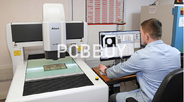
No matter what type of PCBs, they have to go through similar quality inspection methods and items. Based on inspection method, quality inspection items usually include visual inspection, general electrical performance inspection, general technological performance inspection and metalized via inspection.

• Visual inspection
With the help of ruler, vernier caliper or magnifying glass, visual inspection is simple to be carried out. The inspected content includes:
a. Board thickness, surface roughness and warpage.
b. Dimensions of appearance and assembly, especially assembly dimensions compatible with electric connectors and lead rail.
c. Integrity and clearness of conductive patterns and existence of bridging short circuit, open circuit, burr or voids.
d. Surface quality, existence of pit, scratch or pin holes on printing traces or pad.
e. Positions of pad vias and other vias. It should be inspected that whether vias are missed or inaccurately punched, whether via diameter is compatible with design requirement or not and whether there are nodules and voids.
f. Pad plating quality and extent of firmness, roughness, brightness and void of bulge defect.
g. Coating quality. Whether plating flux is even and firm and position correct and whether flux is even and its color meets concerning requirement.
h. Character quality such as whether they're firm, clear and clean with no scratch, penetration or disconnection.
• General electrical performance inspection
There are two kinds of tests under this type of inspection:

a. Connecting performance test. During this test, multimeter is generally applied to inspect the connectivity of conductive patterns with focus on metalized via of double-sided PCB and connectivity performance of multi-layer PCB. For this test, PCBCart provides general inspection before each fabricated PCB leaves its warehouse in order to ensure the implementation of its basic functions.
b. Insulating performance test. This kind of test aims to inspect insulating resistor on the same plane or between different planes in order to ensure the insulating performance of PCB.
• General technological inspection
General technological inspection covers solderability and plating adhesion inspection. For the former, wetting performance of solder to conductive patterns is inspected. For the latter, it can be inspected by qualified tips that are first sticked to plating plane to be inspected and then are pulled off quickly after even pressing. Next, plating plane should be observed to ensure whether fall-off takes place or not. Furthermore, some inspections can be selected based on practical situations such as copper foil anti-falling intensity and metalized via anti-pulling intensity.
• Metalized via inspection
Quality of metalized vias plays a role of extreme significance for double-sided PCBs and multi-layer PCBs. Lots of breakdown happening to electric module or even the whole device lies in quality issues of metalized vias. Therefore, it's quite necessary to pay more attention to the inspection of metalized vias. Metalized via inspection covers the following aspects:
a. Metal plane of via wall should be complete, smooth and void of empty holes or nodules.
b. Electrical performance inspection should be carried out in accordance with short circuit and open circuit of pad and metalized via plating plane, resistance between via and leads.
c. Resistance change rate of vias shouldn't be over 5% to 10% after environmental test.
d. Mechanical intensity refers to adhesive intensity between metalized via and pad.
e. Metallographic analysis test is responsible for inspection in terms of plating plane quality, thickness and uniformity of plating plane, and adhesive intensity between plating plane and copper foil.
Metalized via inspection usually comes in combination of visual inspection and mechanical inspection. Visual inspection is to observe PCB with it placed under the light and complete and smooth via wall is capable of reflecting light evenly. However, via wall containing nodules or voids won't be so bright. For volume manufacturing, inspections should be implemented by on-line inspection equipment such as Flying Probe Tester.
Owing to complicated structure of structure of multi-layer PCBs, once problems are observed in the process of subsequent unit module assembly testing, it's difficult to position breakdowns quickly. As a result, inspection of their quality and reliability has to be very strict. Apart from regular inspection items mentioned above, other inspection items include the following parameters concerning resistance of conductor, resistance of metalized vias, short circuit and open circuit of inner layers, insulating resistance between all lines, adhesive intensity of plating plane, adhesion, anti-heat shock, impact resistance to mechanical shock, current intensity etc. Each index has to be obtained through the application of professional equipment and methods.
Industry Category


