PCB layers
By: 03/11/2021 11:01

Anywhere between 2–40. You can choose the number of layers. There are at a minimum two layers to a PCB, the conducting layer (usually copper but others can be used), and the insulating layer.
With modern Photography methods, the lines that form the conductors can be made very thin. This can make them susceptible to ungluing themselves from the insulating material with excessive amounts of heat.
Along with the insulation or substrate layer, additionally can be the solder mask layer, and finally can be a opaque silk screening on top with the components identified, component layer), also on the back can be another silk screening of paint for the SMT layer.
Then comes multi-layer PCB assignment, and depending on layers complexity goes up.
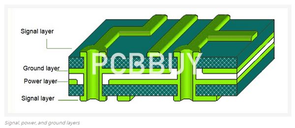
As explained under point 4, the PCB is defined as a number of copper layers in a well-defined sequence. Copper layers are usually just named layers or also called SIGNAL layer. However, to define the complete PCB, other layers are required. they are usually named by their functionality and position. Examples: TOP solder mask layer, TOP paste layer, TOP legend layer, BOTTOM peel-off layer etc…
In general, a PCB assembly is classified by the number of copper layers. Boards that consists of 1 or 2 layers are often called:
1-layer PCB = single sided PCB
2-layer PCB = double sided PCB
Boards with no copper layers or with more than 2 copper layers are defined and called by the number of copper layers.
Industry Category


