PCB panelization guidelines
By:PCBBUY 07/15/2021 17:41

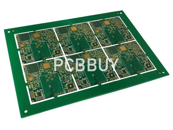
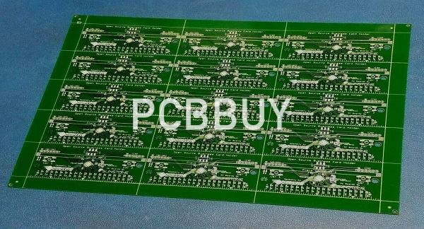
To custom the several types or copies of PCB, PCB panelization is the process of building PCB in large panels of multiple boards. But how to meet the various manufacturing requirements and what is the importance of panelization. Check the content below for more professional knowledge
If you want to order PCB product, please check and custom your order online.
Why we process PCB panelization?
PCB panelization can save money and time
As a result of mass production, PCB panelization enables you to save money and time. The cost of building many boards in large panels of multiple boards is more cost-effective than building them singularly. The core advantage of penalizing several projects is to save money. There are shipping and tooling costs for different projects, and if you have several un-panelized printed boards, it means that you will pay these fees multiple times.
However, if you have multiple projects in large panels on a single printed board, you will pay the fees just once. Since your boards are in large groups and are together, you can ship them simultaneously, which helps save the shipping costs that would occur with separate shipments. By getting all your boards in a single, large panel, it means that the rapid-fire pick and place machine will get all the components of the printed boards at a go. It helps save setup time.
PCB panelization improves work efficiency
As a way of improving the productivity of the PCB manufacturing process, it is common practice to mount several copies of smaller printed circuit boards in a manufacturing panel. It is an effective method of fabricating and assembling the boards instead of building them one by one. The panel must contain the same materials and layer stack-up configuration as the printed board.
It is also essential to choose the size of the panel, whether small or large, that best fits your printed circuit board's needs and the various manufacturing and assembly processes. The more boards you can fit into a PCB panel, the more efficient the manufacturing process will become. It will also reduce the number of panel space that will go to waste.
During panelization, PCB panel designers must use all the arrangement options when placing the PCB designs to optimize the panel space and improve manufacturing efficiency.
PCB panelization improves product quality
PCB panelization is not an optional manufacturing process; mainly, if you produce large quantities of similar circuit boards, you will need to penalize them. Since board uniformity is the goal of panelization, it aids product quality as related components will be placed on different boards at a go. There will be less probability of an error occurring in the manufacturing process when you use penalization. PCB panelization occurs when you produce smaller circuit boards to ensure that the components are similar and uniform. This process helps maintain the quality of the products.
PCB panelization helps designers to get high-quality boards in large numbers. By assembling multiple small PCB, designers will be able to notice missing components and correct errors. It will improve product quality. By contracting your PCB project to a custom PCB manufacturer, your printed boards will meet the excellent industry standards.
Cost-effectiveness of the PCB panel
As a PCB designer, it is essential to know some best manufacturing practices to reduce the cost of PCB. Some manufacturing processes can incur unnecessary charges. Knowing some ways to reduce the PCB costs as much as possible without compromising the quality can be a great way to start.
Panelization affects the cost of PCB when you do it correctly. The higher the volume of PCB copies that you want to produce, the lesser the cost of manufacturing it will incur when you employ panelization techniques.
By employing on-board panelization, you can increase the cost efficiency of your PCB. As a PCB designer, when you frame PCB into panels, they have higher energy and less waste of PCB materials.
Prototype PCB panel can add different designs
PCB designers can make different designs at a go by using panelization techniques. The essence of penalizing a printed board is to replicate the models to fill up the panel space and reduce wastage of materials. As a PCB designer, you can make prototype PCB panels with different designs by arranging the boards to utilize the group's areas. For instance, you can penalize a large L shaped printed board and a small rectangular board in a single panel as long as they have similar components and matching layer stackup configuration.
As a PCB designer, it is essential to put your PCB design tools to ensure that you produce boards that you can penalize effectively. Ensure to consult with your PCB manufacturer in the early stages of the manufacturing process to get the most efficient panel design and avoid the unnecessary costs of redesigning and fixing manufacturing errors.
It protects PCB from vibration and shock
During PCB assembly, various factors affect the PCB, and some include environmental risks like extreme temperatures, humidity, dust, vibration, and shock. To ensure the printed boards' longevity, it is essential to curtail these environmental risks that can lead to PCB problems in the long run.
As a PCB designer, it is essential to know the importance of panelization and how it protects the PCB from shock and vibration during assembly. There are two common ways of penalizing PCB, and they are:
V-groove panelization
This process of panelization involves using a triangular saw to cut about one-third of both sides of the panel, leaving a thin section of FR4 that will hold the PCB. This method allows the use of simple tools to separate each PCB when you want to depanelize it.
However, you cannot make use of v-groove panelization if some components are hanging on the boards' sides. It is to avoid the saw from hitting and destroying the parts of the PCB. One of the advantages of this method is speed. The saw cuts through the sides in a fraction of a second. It also adds small space to the panel's size, which can be a plus and help save on manufacturing costs.
Tab-route panelization
You can use this method for boards with intricate designs and which you cannot separate by simple lines. When the printed boards have multiple layers, this method is your best option. The tab-route panelization process involves using a router to cut through the FR4 boards, leaving small tabs behind. During PCB assembly, you can use simple depanelization tools to break them apart or even use your hands.
One advantage of the tab-route panelization method is that it allows components to overhang the boards' sides. It implies that the parts will not experience damage during the panelization process. By choosing the right panelization method, you can ensure your products' safety by protecting them from vibrations and shock that can cause PCB problems.
Industry Category


