PCB surface finish types and comparison
By:PCBBUY 08/06/2021 17:15
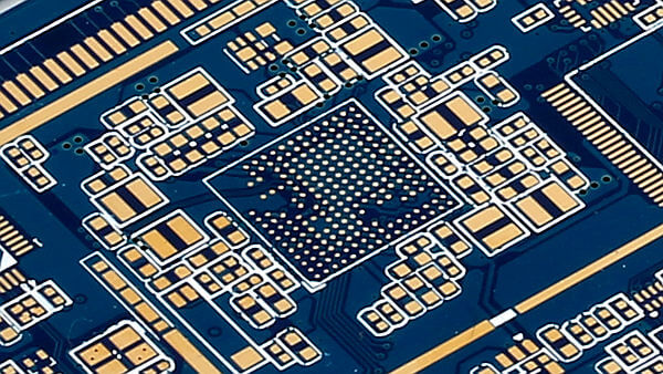
Confronted with so many types of surface finish on PCB pad or land, how should we select the best type of surface finish for our PCBs? This article is a comprehensive guideline for you to refer to. In this passage, we are going to compare the differences of the surface finish types of PCB. Check the content for more professional knowledge about it.
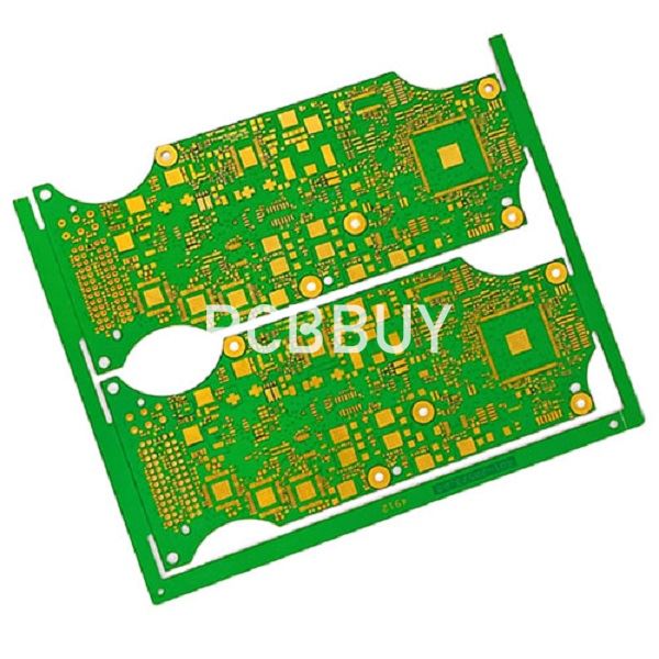
What are the attributes of each PCB surface finish?
OSP
OSP, short for Organic Solderability Preservative, refers to a thin film that is formed at the surface of bare copper in a chemical method. This film features oxidation resistance, thermal shock resistance and anti-wettability, more suitable for developing requirement of SMT in electronic industry.
Here are advantages of OSP surface finish:
1). Suitable for PCB with SMT and fine line space;
2). Capable of stopping copper surface from oxidation, suffering repeated heat shock and compatible with multiple solder and easy for soldering;
3). Beneficial to smoothness of PCB;
4). Environment friendly;
5). Contributive for low cost;
Of course, OSP film is so thin that it's easy to be scratched and engineers have to be very careful since once film is broken, solderability won't be insured.
HASL
HASL, short for Hot Air Solder Leveling, refers to dipping PCB into melting solder bath and then redundant soldering tin is blown away from PCB surface or metalized via through hot wind so that a smooth, uniform and bright soldering tin coating can be obtained. As users' requirement on PCB with flux coating on bare copper increases, HASL receives fast development.
Boards have to meet the following requirement after HASL:
1). All solder coating layers have to be smooth, uniform and bright with no defects such as knot or exposing copper. In addition, soldermask can never suffer from bubbles, falling off or color changing and copper under soldermask should never be oxidized or change color. There shouldn't be foreign matters on the surface of PCB or in via and soldering tin shouldn't be there either.
2). Thickness of soldering tin layer should be in the range from 3μm to 8μm with overall covering soldering tin layer and solderability as principles.
3). Traditional soldering tin layer containing lead is increasingly be cancelled and lead-free soldering tin with tin as core, coupled with infinitesimal copper or nickel. The key is to maintain solderability. Melting point of lead-free solder tin is higher than that with lead by 30°C so heat resistance of substrate material and reliability of through-hole vias on the board will be challenged.
ENIG
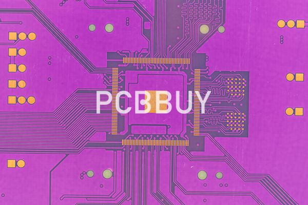
ENIG, short for Electroless Nickel and Immersion Gold, refers to first deposition of nickel layer and then gold layer on copper surface of PCB through chemical electroplating. Chemical nickel player and gold layer have been massively applied owing to their advantages including good dispersibility, solderability, wiring bond performance, soldering performance and their compatibility with all kinds of flux. Compared with OSP and HASL, ENIG is capable of meeting multiple assembly requirements with functions of solderability, connection, wiring and heat dissipation. Moreover, both board surface and SMD pad are smooth, suitable for fine lines.
Immersion gold on nickel surface is actually a replacement reaction. In principle, when nickel surface is totally covered by copper, gold precipitation will stop. However, as a result of too many holes on the surface of gold layer, nickel under gold with multiple holes will still be dissolved and gold will still continue to be precipitated on nickel with an increasingly low speed until it stops.
ENIG is simple to operate without need of technical leads. But black pad will possibly take place in the process of soldering, leading to reliability issue. At present, ENIG is still an important type of surface finish and new nickel coating solution has been developed, which is capable of effectively controlling stability of solution and decreasing brittleness of nickel layer for more flexibility. PH value of new type of immersion gold solution tends to be neutral with gold content greatly decreased, leading to obvious reduction of cost and corrosion.
What are the new types of PCB surface finish?
With PCBs developing towards high density and high performance, some present surface finishes fail to meet all requirements.
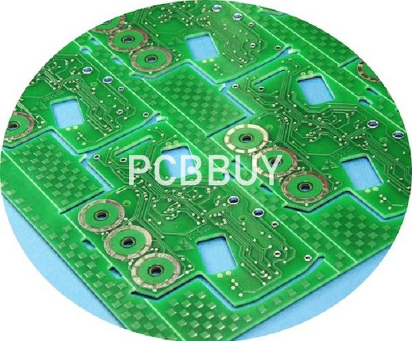
In accordance to the problems occurred by ENIG and ENEPIG, here are some solutions.
EPIG or EPAG
Due to the bad influence of nickel layer on fine circuit and high-frequency signals and nickel's complete inadequacy, thin ENEPIG is applied as a solution to disadvantages of ENIG and ENEPIG. Chemical palladium/gold plating is applied to replace ENIG and ENEPIG. Without the participation of nickel, surface finish becomes so thin that deformation won't be generated to circuit. Moreover, high-speed signal transmission loss is decreased as well.
A variation of ENIG is EPIG (Electroless Palladium/Immersion Gold) whose palladium layer is 0.1μm thick and copper layer 0.1μm thick. Through experiment and test, EPIG is concluded to be with good reliability and expansibility.
Another variation is EPAG (Electroless Palladium/Autocatalytic Gold) with the thickness of palladium layer 0.15μm and copper 0.1μm, suitable for wiring bonding of gold lines and copper lines. Advantages of EPAG include better high-frequency attribute, suitable for fine space circuit as a result of thin coating, reliable soldering or wiring bonding and reduction in procedure and cost.
Electroless nickel ImAg (Ni/Ag)
In spite of low cost and excellent solderability of ImAg, it tends to be easily oxidized owing to its bad anti-corrosion capability. As a result, some improvement has been done with Ni/Ag introduced. Nickel features good conductivity and solderability while nickel has anti-corrosion capability.
With similar technology with ENIG and ImAg, Ni/Ag is developed from practical perspectives. Ni/Ag features palladium thickness in the range from 2μm to 6μm and that of silver 0.1μm.
HASLEN
HASLEN is the combination between HASL and electroless nickel. Usually, nickel is difficult for wetting and plating as a result of oxidation when it's exposed to air, so liquid flux is developed based on DES. Compared with HASL, the advantages of HASLEN include: a nearly unlimited life span as a result of higher anti-oxidation reliability; higher reliability owing to its high temperature resistance; avoidance of black pad; low cost.
SENIG/OSP
Electronic package arouses a lot of requirements on PCB surface finish. Miniature and lead-free trend of electronic assembly put higher requirements on surface finish, which is why SENIG/OSP occurs. This type of technology is complicated in that after the formation of PCB pattern and soldermask pattern, imaging is implemented to protect copper surface for OSP and expose copper surface for ENIG after which photo-induced resistant layer is eliminated to complete OSP. The key point of these technologies lies in corrosion resistance of electroless nickel layer.
Industry Category


