What are the PCB testing methods?
By:PCBBUY 05/10/2021 18:29

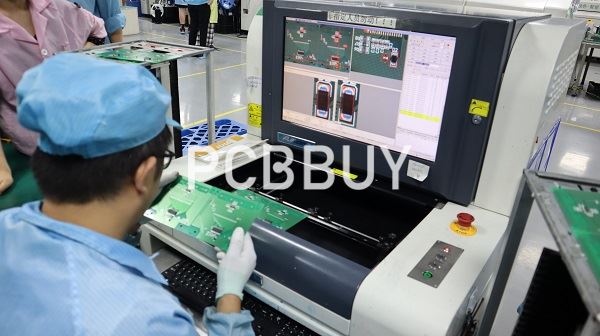
PCB assembly testing methods are an integral part of the manufacturing process. Reputable electronics contract manufacturers (ECM) offer a variety of PCB testing methods, enough that sometimes it’s hard to keep them straight.
Every manufacturing process has an inherent failure rate. Placement of solder outside of the designated location can lead to a solder bridge that might be invisible to visual inspection. PCB testing is crucial to: minimize waste, reduce returned products, and optimize safety.
The application of circuit board testing during PCB manufacturing not only provides a pillar of confidence, but has practical implications as well. Verifying your board’s quality allows you to focus strictly on functional testing during prototyping, enabling to easily transition to production with the assurance that the PCB will perform as desired in the field.
What are the types of PCB testing methods?
There are several PCB available testing methods, each testing method should be considered closely to determine if it meets the specific needs of your manufacturing environment. Some factors to consider include the type of product you’re testing, the problems you’re testing for and the reliability of the test method. we’ve summarized the main qualities of four popular types of PCB testing methods below:
What is ICT?
ICT, also known as In-circuit testing is a popular PCB testing method that many PCB manufacturers prefer to employ, and it can find 98% of faults. The tester system contains a matrix of hundreds or thousands of drivers and sensors, which perform the measurements for the test.
A fixture connects to the in-circuit tester and is the part that interacts directly with the board being tested. This fixture looks like a bed of nails and is designed specifically for the board in question. Fixtures are generally the most expensive part of this system.
Additionally, the cost of the equipment means that this testing method is best suited for the final testing of stable, high-volume products, not for low-volume productions or early testing stages where the design may change multiple times.
What is Flying Probe Test?
The fixtureless in-circuit test (FICT), also known as the flying probe test, is a type of ICT that operates without the custom fixtures, reducing the overall cost of the test.
FICT testing is used for the same things as traditional ICT, but because of the way it goes about testing, it offers different advantages and disadvantages. While FICT is able to adapt to new boards quickly, easily and cost-effectively, with a simple programming change, it tends to be slower than the traditional ICT. This quality makes it an ideal testing method for small-production tests and prototype testing but less effective for large-scale production.
What is Functional Circuit Test?
A functional circuit test is exactly what it sounds like — it tests the function of the circuit. This type of testing always comes at the end of the manufacturing plan, using a functional tester to check whether a finished PCB performs to specifications.
Functional testers usually do so by interfacing with the PCB via its test-probe points or edge connectors and testing to certify that the PCB functions according to design specifications. The test equipment then runs programs to test the PCB, ensuring that the equipment functions exactly as intended. Functional circuit tests are the last type of test to complete in a PCB manufacturing plan, ensuring that the product going out functions according to specifications. Generally, functional circuit tests just look at the product’s functionality as a whole and grade it on a pass or fail basis.
What is Boundary Scan Testing?
The boundary scan test looks at the wire lines on PCBs and is widely used as a way to test integrated circuits when it isn’t possible to reach all the nodes of the circuit. In this type of test, cells are placed in the leads from the silicon to the external pins, testing the functionality of the board.
The big differentiating quality of this type of test is its ability to assess a board without reaching all of its nodes. This quality is an important one for evaluating integrated circuits with multiple layers PCB and high density since these types of PCBs have been becoming more common in recent years.

What are the benefits of PCB testing?
There are many benefits of PCB testing in the manufacturing process. Check out some of the following top advantages of PCB testing:
Bug identification
The primary benefit of PCB testing is that it helps identify problems in PCBs. Whether the issue lies in functionality, manufacturability or elsewhere, PCB tests identify issues in a PCB design so that designers can adjust accordingly.
Time savings:
PCB testing in the early stages can help save time in the long run, allowing designers to identify major issues during the prototyping stage. Thorough testing enables designers to determine the root cause of each problem posed quickly and easily, making adjustments so that they can move on with production at a faster rate and reduce product lead-time.
Cost reduction: PCB testing prevents wasteful production of faulty products by using prototypes and small-scale assemblies to test the products. By completing thorough testing early in the design process, designers can prevent wasteful full-scale assemblies of faulty PCBs, ensuring that the design is as flawless as possible before it goes into production. T
Fewer returned products
When companies conduct PCB testing, they lower the chances of selling defective products or those that don’t meet performance standards. As a result, they don’t see as many returned products, leading to reduced costs associated with refunding customers and handling defective goods.
Increased safety
Since PCBs are often used in essential electronic technologies, their failure can cause major issues for a company’s productivity or an organization’s ability to perform essential services. A defective PCB could cause a fire, potentially putting those near it in danger. Testing prior to manufacturing can also ensure machines and workers aren’t damaged or injured due to an improper design during production.
Industry Category


