PCI Express PCB Layout Guidelines
By:PCBBUY 08/16/2021 17:35

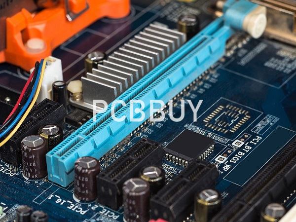
PCI is a popular connection interface used for attaching computer peripherals such as RAM, ethernet, and network cards, I/O cards to a motherboard. It was introduced in 1992 with the aim of supporting complex data transfers and evolved its purpose way beyond the same. The PCI bus was made to be available in 32-bit and 64-bit versions. The PCI technology has undergone various updates to evolve into PCI Express which is still under development.、
In this passage, we will tell you everything about PCI Express and please check and read our content for more professional knowledge.
If you want to order PCB product, please check and custom your order online.
What is the working principle of PCI Express?
PCI Express is a serial connection that works more as a network than as a bus. Instead of one bus handling data from various sources, it includes a switch controlling various point-to-point serial connections. Such connections will spread outward from the switch leading to the devices where the data is required to go. As each device has its own dedicated connection, devices no longer share bandwidth as they do on a conventional bus.
What is the evolution of PCI?
The PCI specification was utilized by the computer industry from 1992 to 2004 as the primary local bus system within a computer. It standardized how PCI expansion cards ranging from a network card to a modem can be self-installed and exchange information with the CPU. CPU processor frequencies rose from 66MHz in 1993 to well over 3GHz in 2003. The existing PCI bandwidth had trouble keeping up with the I/O processing capabilities of the new processors which is what led to the development of PCI Express spec.
From 2004 Intel introduced its PCI express spec which kept the core of PCI’s software infrastructure and wholly replaced the hardware infrastructure that could handle higher I/O requirements of processors. PCI had parallel interconnect whereas the new PCI Express has a serial point-to-point interconnect capable of high bandwidth transfers.
What are the guidelines of PCI Express PCB Layout?
Given are some PCI Express layout and routing guidelines that enable efficient design.
Trace routing specifications
When compared to most high-speed devices available, PCIe generations permit longer trace in their layout routing specs. Every generation comes with its own specifications on impedance and maximum trace lengths for varying data transfer rates. These should be closely followed to obtain the required performance. The exact routing specifications will depend on which PCIe generation you are utilizing for your design.
Trace lengths in Gen 1 and Gen 2 both let RX (received) and TX (transmitted) signal traces reach up to 21 inches in length. When it comes to Gen 3, trace lengths can only go up to 14 inches on signal trace PCIe planes. While each TX trace pair can have only two vias, RX pairs can include up to four vias to maintain impedance within the required specification. A COM Express carrier board allows for trace lengths of up to 9 inches for Gen 1 and 2 when the traces are being sent to a PCIe slot.
The tolerance for differential impedance values also differs among the various PCIe generations and bus standards. The values may be different for each bus and generation combination, but they can be found in the COMCDG Rev. 2.0 specification.
When keeping the impedance of microstrip traces within specified tolerances, you need to use PCB design software to include controlled impedance routing features. The interactive routing tool in the software will ensure your traces are spread out with the right spacing and geometry.
Stack-up and grounding
Standard PCIe boards incorporate a 4-layer stack-up with two interior power planes and two signal layers on each surface. Each power layer can be brought to varying bias levels based on device requirements. Other designs for PCIe boards go for a 6-layer stack-up with two signal layers that run between two power layers. In another scenario, one of the power planes can be replaced with a ground plane. In both cases, you can achieve better immunity to EMI by routing signal traces on the inner layers.
You can even route traces with varying data rates on different layers. For instance, in a mixed-signal board such as the ones in a WiFi device on a PCIe card, you can route digital traces on the outer layers and the RF traces on the inner layers. The ground/power planes will effectively block noise from reaching the sensitive analog signal traces.
Regardless of the stack-up used, you will need to meet the overall board thickness standard of 1.57 mm or 1 mm for PCIe Mini. You will also need to consider standard high-speed design techniques as the Gen 1 of PCIe operates at 2.5 GHz clock speed with future generations increasing in speed.
PCI differential pair routing
Routing around obstructions and component placement and via placement on a PCIe board is really important. There needs symmetric routing to pins, pads, and components along with the BGA breakout routing. Differential pairs need to be tightly coupled throughout their entire length, with variations in one trace due to vias, pads, or components being mirrored in the other trace. This ensures crosstalk is minimized throughout the differential pair length. Similar practices need to be applied while routing BGA breakouts or breakouts from other components.
As the performance requirements of high-speed PCB design continue to increase, it becomes critical to ensure that your design meets PCIe layout routing specifications. PCB board manufacture for PCI requires a great deal of expertise and experience that only a few manufacturers can provide.
Industry Category


