Panelized PCB guidelines
By:PCBBUY 07/08/2021 17:27

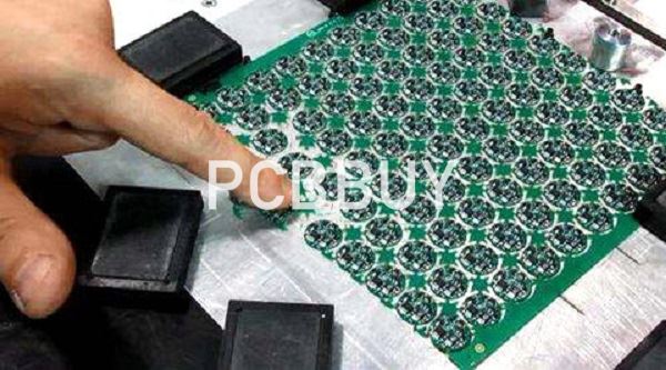
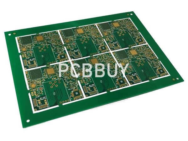
There are several different designs on a single panelized PCB. These sections then break off into different individual boards resulting in inefficient use of space. In this passage we will provide you everything about panelized PCB, come and read the content below for more information.
What to prepare for panelized PCB?
Cost efficiency
This is one of the main benefits of having a PCB panel. If you want to make multiple PCBs, the manufacturer would likely charge more for the additional time they spend to manufacture a higher number of boards.
A panel will have multiples of the same design on a single PCB. This could result in one large board with over 30 designs and has to be made and processed only once instead of making it 30 times on multiple PCBs.
Faster turnaround time
Since many boards can make on a single panel in a single run, this results in a large amount of time-saving for the manufacturer which the result in faster delivery time of your PCB. You are using panel results in a faster time to market for your product.
Convenience factor
Imagine you are working on a device that has one main board and two daughter boards. In a case like this, where your final product has multiple PCBs, It makes more sense to combine all three on a single panel. This also helps in organizing large quantities. Using a panel, you can make sure that all PCBs for a single product are on one panel rather than multiple PCBs scattered all around.
Faster board assembly
When doing board assembly, whether it be a couple of 10s of prototypes or 1000s, time consumed in swapping outboards and putting new boards into your machines causes a loss of productivity.
If you are doing it manually, then it takes a lot of time to align a stencil and then apply the paste to all boards. In situations like these, panels speed up the process. Loading a single panel of multiple boards results in faster production.

What are the design tips for panelized PCB?
V Score or V Groove
Each panel after fabrication, we require a reliable method to separate from each plate. This method should be such that it requires minimal or no tools to separate boards. One such way to do it is by using V Score lines.
V Score lines are the cut line defined on the mechanical layer of the board design. The manufacturer then performs V-shaped cuts on those lines, which go about 1/3rd the board's depth. The next step after this is to physically break off the boards, and they then break off cleanly along the edge where V cut lines exist.
Break off tabs
The second approach to separating individual boards from a panel is using break-off tabs. These are narrowed down areas of the board with many holes or vias drilled into the edge, which is later broken off. On the application of force, the narrow region with the holes breaks off as it is the weakest point on the panel. The only disadvantage of using this approach is that the board edges won't come clean. It is different from when using the V Groove method.
Clearances
Whenever designing a panel, there needs to be a minimum clearance between individual boards on the panel. A board that uses V Grooves would also need some minimum clearance near the cut lines. This value is usually about 2mm and is usually specified on the manufacturer's technical capabilities page. A board that does not have enough clearance may break off in a manner that damages the board's functional section.
Processing tabs
Finally, on certain boards or panels that are very small, there needs to be a blank region added so the factory's machines can process the entire board. This is a blank region added to the design, so the board meets the minimum size requirements. Often this is done by the factory, but sometimes you may need to define a blank region along with cutting lines in your CAD software.
What are common products for panelized PCB?
Products with multiple boards
Many products these days contain multiple boards. These can be large appliances like inverters and microwaves where you have a separate power and control board or a product like a game console with daughter boards. It's common to consolidate all the different boards onto a single panel before you send out for manufacturing in these cases. This method helps keep things organized and numbers easy to track
PCBs with small physical dimensions
Many products have very small PCBs. These can be devices like cell phones or adapter boards for microcontrollers and so on. In such cases, getting multiple small PCBs made would be more expensive than just getting a panel made, which contains many of these smaller boards. Many times, in the case of very small designs, 100s of boards can be made on a panel for less than 10$. This is extremely helpful for prototypers and hobbyists.
Designer Products made out of PCBs
These days there is an increasing trend to make products such as business cards, badges, and rulers out of PCBs. In these cases, it makes sense to build a large panel with multiples of these designs. There are two reasons for this.
1. The individual boards are usually too small to manufacture independently
2. The overall price is lower when using a panel
Also, these products are usually mass-produced, so using a panel becomes very convenient and economical. It's common to be able to fit up to 30 Business cards onto a single panel.
Industry Category


