Parasitic Capacitance in PCB
By:PCBBUY 08/16/2021 17:30

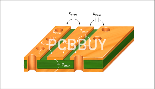
Parasitic capacitance or stray capacitance is the result of a virtual capacitor formed between two traces separated by a dielectric. It occurs due to the potential difference generated when the current-carrying traces run in close proximity. To learn more, read the role of trace current capacity in PCB design.
This effect is even possible if the conductors are appropriately insulated. It is not possible to avoid parasitic capacitance since no electrical circuit is ideal. In this passage, we provide all about parasitic capacitance in PCB please check and read the content below.
If you want to order PCB product, please check and custom your order online.
How to calculate parasitic capacitance in PCB?
Parasitic capacitance is an inherent property of the conductors. It is the storage of per unit change in electric potential. The parasitic capacitance is calculated as C= q/v. Where C is the capacitance in farads, v is the voltage in volts, and q is the charge in coulombs.
· For a constant electrical signal that does not change over time, dv/dt = 0 which means, no change in potential; hence i =0.
· If there is a capacitor in the circuit loop, dv/dt will converge to a fixed value, i.e., change in potential, resulting in a current flow; hence i ≠ 0.
Trace capacitance calculation
The capacitance of a parallel plate capacitor is given by C= (kA/11.3d)pF. Where C is capacitance, A is the plate area in cm2, k is the relative dielectric constant of board material, and d is the distance between the plates in cm.
What is the effect of parasitic capacitance in PCB?
The parasitic capacitance effect is a matter of concern in high-frequency circuit boards. While operating at low frequencies, parasitic elements can be ignored since they do not really impact system functionality. Every pad in a circuit board has its parasitic capacitance, and every trace has parasitic inductance. Pads also add their parasitic resistance that stimulates IR losses. Parasitic capacitance can exist between conductors on PCBs, bare boards, PCBAs, assembled boards, and within component packages, especially surface mount devices (SMDs).
Since intrinsic capacitor plates have a potential difference, there is a chance of current flow. It does not matter whether the charges are stored between the capacitor plates; the current will not flow until there is a potential difference. As soon as this potential difference increases, a corresponding decrease in electron flow towards the load can be observed for the desired signal path that negatively impacts signal integrity.
What are the differences between parasitic capacitance and stray capacitance?
The term stray capacitance is often used interchangeably with parasitic capacitance. However, parasitic capacitance accounts for the fact that it will hamper the circuit operation, while stray capacitance accounts for how unwanted capacitance is introduced.
What is stray capacitance?
Stray capacitance doesn’t always get induced due to the virtual capacitance formed between two PCB conductors but also due to the effect of the surrounding environment. Hence, it is termed as stray capacitance.
What is parasitic resistance in a PCB?
Parasitic resistance exists in series along traces or as a shunt between the conductive elements.
What is parasitic inductance in a PCB?
Parasitic inductance exists along a trace and exhibits the behavior of storing and dissipating electrical energy, like an actual inductor. All conductors are inductive, and at high frequencies, the inductance of even relatively short pieces of wire or PCB traces may be important.
Where R is the wire radius, and L is the length.
How to find the inductance of a PCB trace?
Trace inductance increases with trace length and lack of ground plane.
What are the causes of parasitic resistance in PCB?
At high-frequency, current flow in a circuit board is affected by the parasitic capacitance. Since capacitors are tend to become conductors when frequency increases. Note that when frequency increases, the capacitor will act as a resistor of very small value (approaches to a short circuit), resulting in excessive current flow.
Zc = 1/2πfc ; fc = 1/ωc therefore, as frequency increases, Zc also increases.
Parasitic capacitance can give you chills during high-frequency operation since a capacitor acts like a wire at an infinite frequency. This is the reason why it can accidentally connect the reference plane of any PCB board to the chassis.
Parasitic capacitance effects could be crosstalk and noise, undesirable feedback from the output, and the formation of resonant circuits. So, it is essential to give attention to the overall PCB design, specifically to the layout. A good layout should take utmost care while placing a conductive body by the side of another conductive body.
Parasitic elements include inductors formed by package leads, long traces, pad-to-ground, pad to power plane, and pad to trace capacitors, including interactions with vias, etc. Understand parasitic elements as parasites, a threat to your circuit performance.
Industry Category


