Principles used in PCB Shielding
By:PCBBUY 08/30/2021 09:29
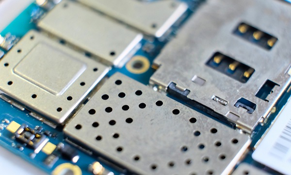
As a pretty important process of PCB manufacturing, shielding plays an essential role. Do you know the principles of PCB shielding? We will talk about the basics of electromagnetic compatibility (EMC) shielding. Please check and read the content below for more information.

How to improve the PCB shielding principles?
Miniaturization of handsets and other wireless devices creates scores of shielding challenges as high-frequency components become more closely spaced. As printed-circuit boards (PCBs) shrink, new electromagnetic-interference (EMI) shielding solutions must provide greater levels of interference suppression, but without significantly adding mass, weight, and cost to a device. Fortunately, a new shielding technology developed by W.L.
Both try to create a complete shield around the PCB's components to ensure proper electrical performance and comply with regulatory requirements for EMI emissions and susceptance.
The goal of an EMI shield is to create a Faraday cage around the enclosed RF components using the six sides of a metallic box. The top five sides are created using a shielding cover or metal can, while the bottom side is achieved by using the ground plane within the PCB quote. In an ideal enclosure, no emissions would enter or exit the box. In reality, leaks do occur, such as from holes perforated into soldered cans that allow thermal heat transfer during solder reflow. Leaks can also occur from imperfections along an EMI gasket or solder attachments.
What are methods of PCB shielding principles?
Shielding a design requires that it be encapsulated on both sides with a layer of material that acts as a barrier to the absorption or radiation of EMI. These layers are connected to ground so that any EMI is harmlessly dissipated.
There are additional considerations that must be factored in when choosing a shield method and material.
Bend Requirements
Each shielding method adds different amounts to the overall thickness of the flexible circuit. As the minimum bend capability is a function of the thickness, it will reduce or limit the bend capabilities of a design. The minimum bend radius and type of bend requirement of shielded designs needs to be accurately defined and reviewed as part of the design and material selection process.
The type of bend requirement static or dynamic, places further constraints. A dynamic bend flex PCB application has a much larger minimum bend capability than that of a static bend design.
Controlled Impedance
Controlled impedance signal requirements place further limitations on the shielding method that can be used. The shield(s) require electrical characteristics that satisfy both the EMI requirements as well as perform as reference planes to achieve the required controlled impedance values. Not all shielding methods can satisfy both.

What are the considerations of PCB shielding principles?
Fortifying electronics against EMI needs to be part of the overall design of the circuit board. Here are the four main areas of PCB layout that should be considered for EMI prevention:
Board Layer Stackup
How the layers are configured in your PCB stackup is an essential first step in the control of EMI. While it may seem attractive to reduce the layer count to reduce manufacturing expenses, that strategy may damage the signal integrity of the board. High-speed signals, sensitive analog nets, and noisy power circuitry all need to be isolated from each other, and that may require additional layers in the stackup. It is also important to provide enough layers for ground planes to shield these signal layers from emitting or being victimized by EMI.
Component Placement
How components are placed will also make a big difference in how the board is shielded against EMI problems. Here are some general guidelines to keep in mind:
· Keep the analog circuitry separated from the digital circuitry.
· Keep your analog components placed closely together to keep their trace lengths short.
· Provide enough bypass capacitors to ensure a clean power delivery network.
· Include low-pass filtering in your design.
To ensure that your design is EMC compliant, it is important to keep PCB components grouped according to their function. You don’t want digital circuitry to flow through an analog portion of the board, except for those signals that directly connect the two together.
Trace Routing
With good component placement, you will already have the foundation necessary for the best trace routing. However, it is still important to follow these routing guidelines to minimize EMI:
· Keep analog and digital signals separated from each other, and isolate sensitive signals from other routing.
· Keep analog routing short and make sure that the signals have clear return paths on their reference plane.
· Use guard traces to prevent crosstalk between two parallel analog traces if you don’t have enough room for the wider spacing. Guard traces also help in shielding between an analog and digital trace, if required.
· Use vias to form a shielded border or fence between functional partitions of circuitry from each other. Via fences are effective and easy to put in, but the trade-off is that they use up a lot of real estate on the circuit board.
Industry Category


