Rigid-Flex PCB Bend Radius Rules to Avoid Trace Cracking
By:PCBBUY 10/28/2026 15:16
Introduction
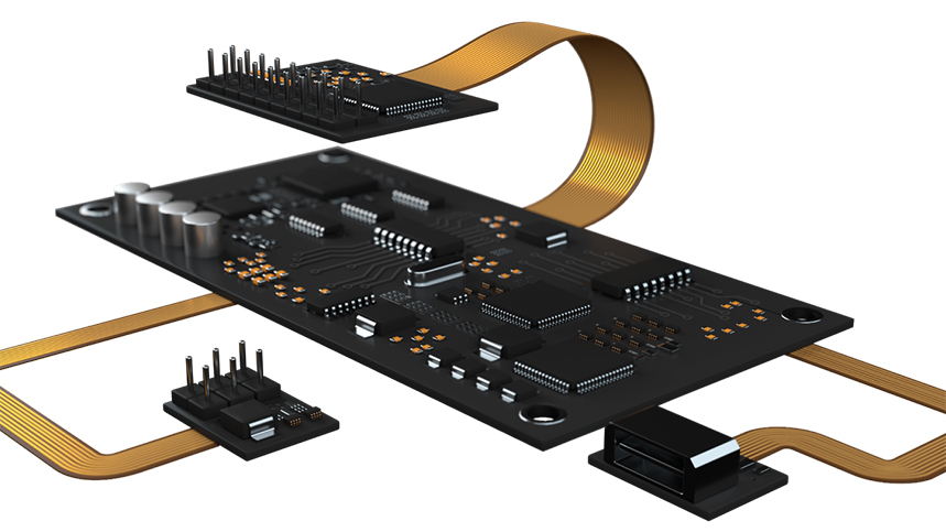
Rigid-flex PCBs combine rigid circuit sections with flexible interconnects, allowing electronic assemblies to fit compact enclosures while reducing the need for cables and connectors. However, repeated or excessive bending can place mechanical strain on copper conductors, leading to trace cracks, intermittent connections, or eventual circuit failure.
Understanding rigid flex PCB bend radius rules to avoid trace cracking is essential when designing electronics for automotive systems, industrial control, power equipment, energy storage, and robotic applications. A reliable design must consider not only the bend radius, but also the flex-layer thickness, copper type, trace routing, and whether the board bends once during installation or repeatedly during operation.

1. Choose the Bend Radius Based on Flex Thickness
Bend radius is generally specified as a minimum radius for the flexible section. A larger radius creates a gentler bend and usually reduces strain on the copper.
The first step is to distinguish between two applications:
-
Static bend: The flexible section is bent during installation and then remains in a relatively fixed position.
-
Dynamic bend: The flexible section repeatedly bends during normal operation, such as in a moving mechanism or robotic joint.
Dynamic applications typically require a substantially larger radius and more careful material selection because copper fatigue accumulates over repeated cycles.
The following values are preliminary engineering guidelines, not universal acceptance limits.
|
Flex construction |
Static bend: preliminary reference |
Dynamic bend: preliminary reference |
|
Single-layer flex |
Approximately 6–10 × flex thickness |
Often 100 × thickness or more |
|
Double-layer flex |
Approximately 10–20 × flex thickness |
May require 100–150 × thickness or more |
|
Multilayer flex |
Often 20 × thickness or more |
May require 200 × thickness or more |
Actual requirements vary with copper type, layer arrangement, adhesive and coverlay construction, neutral-axis location, and required bend-cycle life. These ranges should not replace a manufacturer-reviewed design rule or the applicable customer specification.
For example, if a flexible section is 0.20 mm thick and the design uses a preliminary static-bend factor of 10, the corresponding reference radius is 2.0 mm. This is only an initial design estimate; the actual minimum must be validated against the complete flex construction and mechanical requirements.
2. Route Traces to Reduce Copper Stress
A suitable bend radius alone cannot prevent every trace crack. Routing geometry and copper distribution also affect where strain concentrates.
Route Traces Across the Bend Appropriately
Where practical, route conductors approximately perpendicular to the bend axis. Avoid diagonal routing across the bend when it creates uneven mechanical loading, and use smooth curves rather than sharp corners in the active flex region.
For two-layer flexible sections, offset conductors on opposite layers where the electrical design permits. Directly overlapping traces can create locally stiff regions and concentrate strain during bending.

Keep Vias and Components Out of Active Bend Zones
Plated holes, vias, component pads, and solder joints create local stiffness and potential stress concentrations. Keep them outside the active bend region wherever possible.
The required clearance from the bend and rigid-to-flex transition depends on the construction and geometry. Define these keep-out zones in the fabrication data and mechanical drawing, and confirm them with the manufacturer rather than relying on a universal clearance value.
Select Appropriate Copper and Plane Structures
Rolled-annealed (RA) copper is commonly considered for flexible circuits because of its ductility. The suitable copper type and thickness depend on whether the application is static or dynamic and on the electrical current requirements.
Solid copper planes can reduce flexibility. Where electrical and signal-integrity requirements permit, a cross-hatched copper structure may help improve flexibility. However, any plane modification must be evaluated for grounding, shielding, impedance, and current-carrying performance.
3. Key Design Rules at a Glance
|
Design factor |
Recommended practice |
Risk if overlooked |
|
Bend radius |
Set from flex thickness, layer count, and bend-cycle requirements. |
Excessive copper strain and fatigue cracking. |
|
Trace direction |
Route across the bend approximately perpendicular to the bend axis. |
Uneven strain distribution. |
|
Trace geometry |
Use smooth curves and avoid sharp corners in the flex region. |
Localized stress concentration. |
|
Via and pad placement |
Keep vias, plated holes, and components outside active bend areas where possible. |
Cracking, delamination, or joint damage. |
|
Copper arrangement |
Stagger traces across layers where practical; review solid copper planes. |
Local stiffness and concentrated bending stress. |
|
Rigid-to-flex transition |
Define transition geometry and keep the bend away from abrupt stiffness changes. |
Trace damage or coverlay separation near the transition. |
|
Material selection |
Review copper type, flex dielectric, adhesive, and coverlay together. |
A stack-up that cannot meet the required bend life. |
4. How PCBBUY and PCBBUY Can Support Rigid-Flex Design
For customers developing automotive electronics, industrial control equipment, power systems, energy storage products, new-energy devices, and embodied robotics, rigid-flex design should be reviewed jointly with the mechanical layout and manufacturing process.
PCBBUY can help coordinate the customer's application requirements with PCBBUY's engineering review. PCBBUY's broader PCB manufacturing capabilities include multilayer PCB production, HDI processing, fine-line fabrication, and material selection for specialized PCB applications. However, these general capabilities should not be interpreted as confirmation that every rigid-flex construction, copper type, or dynamic-bend requirement is supported.
Before quoting a rigid-flex project, the engineering team should confirm:
-
The complete rigid-flex stack-up, including copper, dielectric, adhesive, and coverlay thicknesses.
-
The flex-zone outline, bend radius, bend angle, and installation geometry.
-
Whether the bend is static or dynamic, including the expected number of cycles and operating conditions.
-
Trace routing, via and component keep-outs, and rigid-to-flex transition details.
-
Required electrical performance, inspection criteria, and reliability verification.
This review helps determine whether the proposed construction is compatible with the mechanical requirements and whether a different layer arrangement, thinner flex section, or larger bend radius is necessary.
5. Inspection, Reliability, and Shipment Acceptance
Rigid-flex PCB acceptance should be based on the approved fabrication drawing, stack-up, and project-specific requirements. Visual inspection and electrical testing are useful, but neither alone proves that a board will survive its intended bending life.
For applications with repeated motion or demanding reliability requirements, the qualification plan may need to include continuity monitoring during flex cycling, resistance checks before and after cycling, or other agreed mechanical and electrical tests.
Before production, customers and manufacturers should define the inspection scope, applicable acceptance criteria, required test conditions, and documentation package. Shipment records should correspond to the approved revision and the agreed test requirements. Where dynamic bending is critical, qualification evidence should reflect the actual flex construction and intended service conditions.
Conclusion
The most effective way to prevent trace cracking in rigid-flex PCBs is to design the bend around the complete mechanical and electrical requirements. A suitable bend radius, appropriate copper selection, smooth routing, carefully positioned vias, and a well-designed rigid-to-flex transition all contribute to reliability.
By involving PCBBUY and PCBBUY early, customers can review the proposed stack-up, clarify bend-cycle requirements, and establish suitable manufacturing and verification criteria before production begins.
FAQ
1. What is the minimum bend radius for a rigid-flex PCB?
There is no single minimum for every design. The required radius depends on flex thickness, copper-layer count, material construction, and whether the bend is static or dynamic. A manufacturer-reviewed design rule should be used for production.
2. Why do traces crack in rigid-flex PCBs?
Common contributing factors include an excessively tight bend, repeated bending beyond the design limit, unsuitable copper construction, sharp trace corners, vias in the active bend area, and stress concentration near rigid-to-flex transitions.
3. Is dynamic bending more demanding than static bending?
Yes. Dynamic bending repeatedly strains the copper, so fatigue resistance and cycle life become critical. Dynamic applications generally need a larger bend radius and more careful flex-material and stack-up selection than installation-only bends.
4. Should vias be placed in the flexible region?
Vias and plated holes should generally be kept out of active bend zones because they create local stiffness and potential failure points. If placement is unavoidable, the structure requires specific engineering review and validation.
5. Can PCBBUY guarantee that a rigid-flex PCB will not develop trace cracks?
No design or manufacturing process can guarantee zero failures under every condition. The appropriate approach is to review the construction and intended bending conditions, confirm manufacturability, and agree on suitable inspection and reliability tests before production.
Industry Category