Rigid-flex PCB Design Guidelines
By:PCBBUY 09/09/2021 10:03

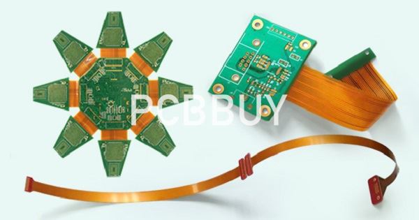
A rigid flex PCB is a combination of both rigid and flexible substrates. One or more flexible circuits are used to connect subcircuits on rigid PCBs. Rigid flex PCBs are usually produced with flexible polyimide material on copper cladding substrate and connects to the rigid FR4 board. The flexible part of the rigid flex PCB usually features a multilayer built with padded through holes securing the interconnectivity between layers.
If you are curious about the design process of rigid-flex PCB, please check and read the content below for more professional knowledge of it.
If you want to order PCB product, please check and custom your order online.
What are the benefits of rigid-flex PCB?
Designing a rigid flex PCB is considerably more challenging than conventional rigid PCB. However, there are good reasons why rigid flex is used in some designs, particularly one that involves fitting the board in tight spaces.
Increase reliability
Connectors serve their purpose when there’s a need to remove the wire harness from the PCB routinely. For a design that involves multiple interlinking subcircuits in an enclosure, adding connectors to the PCB only increases the risk of failure.
Space saving
Often, the designs that call for a rigid flex PCB is one where space is a luxury. For example, handheld thermal scanners can benefit from a rigid flex PCB design as there isn’t much space to fit in wire harnesses and high profile connectors. Instead, with the interconnecting circuit built-in on the flexible substrate, you’ll have more space to route the traces around.
Reduce cost
Rigid flex PCBs are generally cheaper than their rigid counterparts, as the former is harder to produce. However, using rigid flex PCBs may reduce the overall cost of the product. As wired interconnects are replaced by the conductive layers of flexible material, you’ll save on the cost of assembly, which in some cases, involves manual labor.
Ease of testing
It is also easy to automate testing of a rigid flex PCB as all the subcircuits are already interconnected when the PCB is manufactured. The ability to eliminate connectivity issues before the components are assembled, further, prevent unnecessary wastage and expenses.
What are the guidelines of rigid-flex PCB design?
Broadly speaking, a rigid flex design will closely resemble a hardboard design, with the flexible layers fully extending into the rigid areas of the board. Similarly to hardboard layouts, a rigid flex fabrication package will include Gerber layers, along with drill files, solder mask layers, nomenclature, perimeter/rout files, cover layer, etc.
However, there are some key differences between the fabrication packages for rigid flex PCB’s and hardboard applications:
· A rigid flex print generally has many more dimensions on it, and should carefully define the requirements, as these boards are generally used in 3D applications. It should also accurately define the rigid to flex transition areas, as these are not always apparent when viewing the Gerber layers alone.
· The material layup in rigid flex boards is critical, and should be worked out in collaboration with your fabricator. Your fabricator can help you make the right choices in materials based your requirements such as UL flammability rating, minimum bend radii required, mechanical considerations, impedance control on both flex and rigid layers, RoHS certification, lead free assembly compatibility, and other considerations.
· Rigid flex boards usually require additional layers in the Gerber files. Layers 1 and X will have solder mask layers, but you will also need artwork layers that define the coverlayer and bondply sections (if required) of the board, and how much each go into the hardboards. IPC 2223 recommends 0.100″ but your fabricator may be able to accommodate less than that.
What is the future of rigid-flex PCB design?
There are many new designs being manufactured with substantially higher flex layer counts. Some more prevalent designs include those with blind and buried via structures, integrated ZIF connections, and even designs with components mounted into both the flexible areas and the rigid sections.
Some rigid-flex printed circuit board (PCB) designs may have flex areas that require shielding for Electromagnetic Interference (EMI) or Radio Frequency (RF) considerations. There are also designs that have varying thicknesses between the different rigid areas as well as asymmetrical constructions.
This article covers some of the more common types of configurations and combinations that have been generating interest among OEMs. However, there are many additional configurations and combinations available for flex and rigid-flex circuit board stack-ups. The more advanced constructions covered here include odd layer count constructions, asymmetrical constructions, varying flex layer count designs, integrated ZIF connections, blind and buried vias, air gap flex layer constructions, multiple rigid area thicknesses, and shielded flex layers.
Industry Category


