Rigid flex PCB Design Guidelines
By:PCBBUY 09/02/2021 09:21

When you begin to design your rigid flex PCB, there are a few rules you want to adhere to as best as possible. Try to keep the flex layers to a minimum of two for increased mechanical flexibility and reduced costs. In this passage, we will provide the guidelines of rigid flex PCB design, if you are going to learn more about it, please check and read the content below for more.
What are the guidelines of rigid flex PCB design?
Broadly speaking, a rigid flex design will closely resemble a hardboard design, with the flexible layers fully extending into the rigid areas of the board. Similarly to hardboard layouts, a rigid flex fabrication package will include Gerber layers, along with drill files, solder mask layers, nomenclature, perimeter/rout files, etc.
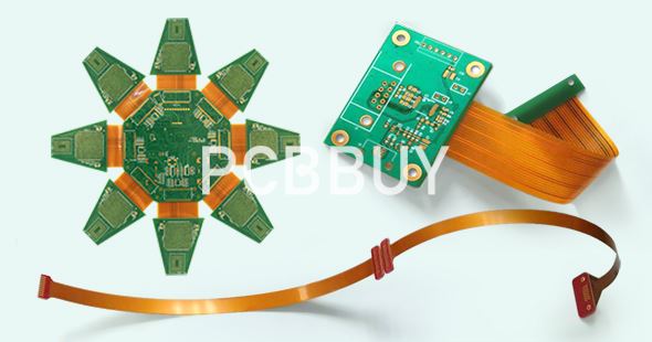
Avoid placing pads and vias on the bending area of the flex part of a PCB. Areas near the bending line will deliver mechanical stress that could jeopardize the structure of the plated holes.
Pads and vias can be placed on areas that are not subjected to bending, although it’s not recommended. In such cases, use anchors to strengthen the plated holes. Additionally, use a teardrop to connect the trace to the plated hole for stronger joints. It’s also a good practice to use larger pads and vias.
However, there are some key differences between the fabrication packages for rigid flex PCB’s and hardboard applications:

· A rigid flex print generally has many more dimensions on it, and should carefully define the requirements, as these boards are generally used in 3D applications. It should also accurately define the rigid to flex transition areas, as these are not always apparent when viewing the Gerber layers alone.
· The material layup in rigid flex boards is critical, and should be worked out in collaboration with your fabricator. Your fabricator can help you make the right choices in materials based your requirements such as UL flammability rating, minimum bend radii required, mechanical considerations, impedance control on both flex and rigid layers, RoHS certification, lead free assembly compatibility, and other considerations.
· Rigid flex boards usually require additional layers in the Gerber files. Layers 1 and X will have solder mask layers, but you will also need artwork layers that define the coverlayer and bondply sections (if required) of the board, and how much each go into the hardboards. IPC 2223 recommends 0.100″ but your fabricator may be able to accommodate less than that.
· Pay Attention to Routing Across the Bending Area. Traces across the bending line should be kept as straight, perpendicular lines. It’s better to use narrower traces that are spread evenly across the flexible area. Adding in dummy traces can help to increase mechanical sturdiness that protects the traces from breaking. For a double layer design, traces should be routed alternately on both the top and bottom layer.
· Avoid Plated Through Holes on the Bending Areas. Avoid placing pads and vias on the bending area of the flex part of a PCB. Areas near the bending line will deliver mechanical stress that could jeopardize the structure of the plated holes. Pads and vias can be placed on areas that are not subjected to bending, although it’s not recommended. In such cases, use anchors to strengthen the plated holes. Additionally, use a teardrop to connect the trace to the plated hole for stronger joints. It’s also a good practice to use larger pads and vias.
The IPC-2223 Sectional Design Standard for Flexible Printed Boards is an excellent resource for wise practices in both flexible circuit and rigid flex circuit design.

What are the advantages of rigid flex PCB design?
By combining the properties of rigid and flexible PCBs, rigid-flex PCBs come with a host of benefits for both manufacturers and consumers.
· Mechanical stability- Their basic structure consists of interchanging layers of rigid and flexible PCBs. This ensures that they're both stable and flexible, facilitating easy installation in small spaces.
· Connection reliability- With rigid-flex PCBs, you get greater stability and polarity, making connections easier and more secure with other components. You will also require fewer connector components with each application.
· Dynamism- Along with repeatability and precision, you'll enjoy greater flexibility with packaging.
· Cost-effective- By using rigid-flex PCBs, you can cut down on the total expenditures.
· High-density applications- Arguably, the best benefit of rigid-flex PCBs is that they can be used for a high-density device population. This is due to their flexibility, stability, and low space use.
· High shock and vibration resistance- Electronic components are used in a wide range of items, some of which experience constant vibrations. With such devices, you won't have to worry about damage as rigid-flex PCB is highly resistant to shock and vibration.
Rigid PCBs offer the advantages of cost containment for high-volume manufacturing tasks, shorter lead times, and decreased installation costs when moving from board design to product release. The decreased production costs exist because of material selection, component and design technologies, the reduced number of holes, surface finish requirements, solder mask requirements, testing parameters, and lower environmental impact. Of those factors, the laminate is the largest cost component.
Industry Category


