Rigid flex PCB manufacturing process
By:PCBBUY 08/05/2021 17:36

In this passage, we are going to provide the details of rigid flex PCB manufacturing process. If you are going to learn more professional knowledge, check the content below for more information.
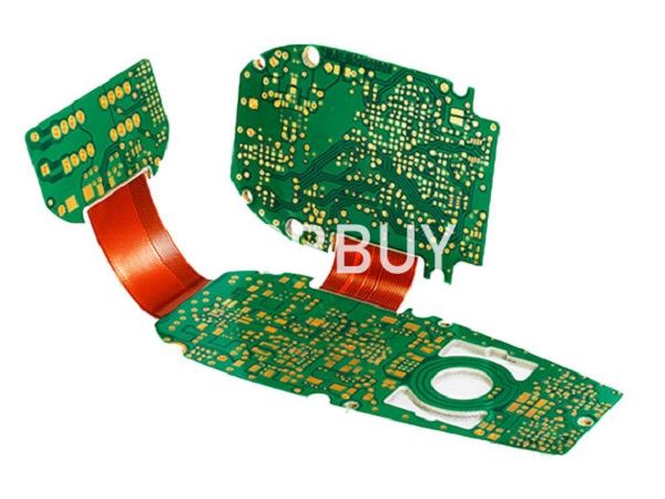
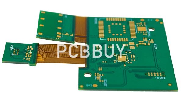
The rigid-flex PCB manufacturing process is time consuming and laborious when compared to traditional rigid board fabrication. It involves several steps that must be carried out with extreme accuracy. Mishandling or misplacing any of the flexible components in the board affects the efficiency and durability of the final assembly substantially.
What are the features of rigid flex PCB?
Due to development trend of aerospace products including light weight, miniaturization, multifunction and assembly densification, higher requirement has been set up for Printed Circuit Board (PCB) technology and manufacturing process. Flexible PCBs are a type of circuit boards that are made of flexible substrate material and feature more advantages than ordinarily rigid PCBs:
• Lower thickness
• Lighter weight
• Dynamically bendable
• Accessible for 3D interconnection assembly
• Higher freedom on electronic design and mechanical design
• More space saving
How to select materials for rigid flex PCB?
Manufacturing technologies of flex-rigid PCBs differ from each other in accordance with different types of PCB boards and the essential technology leading to the differences is fine circuit manufacturing technology and microvia manufacturing technology. As electronic products tend to develop towards light weight and miniaturization, multifunction and assembly densification, advanced PCB boards attracting the most attention include HDI flex-rigid PCBs and embedded flex-rigid PCBs.

What is the manufacturing process of rigid flex PCB?
Rigid-flex circuit board manufacturers assemble the boards by following the steps listed below.
1. Preparing the Base Material – The first step involved in the board fabrication is preparing/cleaning the laminate. The laminate, which contains copper layer – with adhesive or adhesiveless coating – must be cleaned thoroughly before processing with other fabrication processes. This pre-cleaning is important because, copper coils are normally offered by vendors with anti-tarnish features to provide oxidation protection. However, this coating poses a hindrance to rigid-flex PCB manufacturing, hence must be removed.
2. Circuit Pattern Generation – Generating circuit patterns is the next step followed by the laminate preparation. Nowadays, this circuit pattern exposure is done using two main techniques, such as:
• Screen Printing – This technique is popular as it can generate the required circuit patterns/deposits directly onto the surface of the laminate. The total thickness is not more than 4–50 microns.
• Photo Imaging – Photo imaging is the oldest, but still the most popularly used technique for depicting the circuit traces on the laminate. In this method, a dry photoresist film consisting of the desired circuitry is placed in close contact with the laminate. This assembly is then exposed to UV light, which helps transfer the pattern from the photomask to the laminate. The film is then chemically removed, leaving behind the laminate with the desired circuit pattern.
3. Etch the Circuit Pattern – Following the circuit pattern generation, next is etching the copper laminate containing the circuit pattern. Rigid-flex manufacturers either dip the laminate in an etch bath, or it is sprayed with an etchant solution. Both sides of the lamination are etched simultaneously to achieve the desired results.
4. Drilling Processes – Now, the time is for drilling required number of holes, pads, and vias. High speed drilling tools are used to make precision holes. To create ultra-small holes, rigid-flex circuit boards manufacturers use laser drilling techniques. Usually, Excimer YAG, and CO2 lasers are used to drill small and medium holes in the substrate.
5. Through-hole Plating – This is one of the crucial steps in rigid-flex PCB manufacturing process that must be carried out with extreme precision and care. After holes with required specifications are drilled in, they are deposited with copper, and chemically plated. This is done to form layer to layer electrical interconnection.
6. Apply Cover lay or Covercoat – It is crucial to protect the top and bottom side of the flex circuit by applying a cover lay. This is done to provide comprehensive protection to the circuit from aggressive weather conditions, harsh chemicals, and solvents. In most cases, manufacturers use a polyimide film with adhesive as a cover lay material. Cover lay material is imprinted onto the surface using screen printing, which is then cured with UV exposure. In order to ensure proper adhesion of the cover lay material on to the substrate, cover lays are laminated under specified limits of heat and pressure. Unlike the cover lay material, which is a laminated film, covercoat is a material that is literally applied onto the surface of the substrate. The decision regarding the type of coating must be made after considering the manufacturing methods, materials used, and the application areas. Both cover lay and covercoat augment the electrical integrity of the entire assembly.
7. Cutting out the Flex – Blanking or cutting the individual flex board from the production panel is yet another important step that must be executed with caution. When producing rigid-flex PCBs in high volume, manufacturers usually choose the hydraulic punching method. However, the same is not chosen for prototyping or small production runs due to the high tooling cost involved. When creating prototype rigid-flex PCBs in small production runs, a specialized blanking knife is used.
8. Electrical Testing and Verification – The last and final stage in rigid-flex circuit boards manufacturing is testing and verification. The boards undergo stringent electrical testing for continuity, isolation, circuit performance, and quality against the design specifications. Several kinds of testing methods are used, including grid and flying probe test methods.
Industry Category


