
How Should Engineers Select Low-Loss PCB Dielectrics for High-Speed Signals?
By:PCBBUY 09/21/2026 14:50
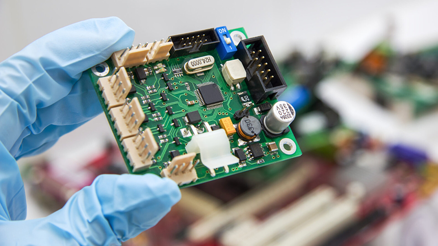
As data rates increase, signal integrity becomes more sensitive to PCB material properties. In high-speed applications, inappropriate dielectric materials can increase insertion loss, distort signal waveforms, and reduce the available design margin. Therefore, low loss PCB dielectric selection for high speed signals should be considered together with transmission-line geometry, copper roughness, stackup design, and manufacturing capabilities.
However, selecting the lowest-loss material available is not always the most practical solution. Engineers must balance electrical performance, thermal reliability, mechanical stability, manufacturing compatibility, and total cost.
For applications such as automotive electronics, industrial control systems, power equipment, energy storage systems, and embodied robotics, a reliable material selection strategy is essential for achieving stable performance throughout the product life cycle.
1. Why Does Dielectric Selection Matter for High-Speed Signals?
A PCB transmission line experiences both dielectric loss and conductor loss. Dielectric loss is primarily related to the material’s dissipation factor, while conductor loss is influenced by copper resistivity, skin effect, and copper surface roughness.
As signal frequency and transmission distance increase, dielectric loss can become a major factor affecting channel performance. Excessive loss may lead to:
-
Higher insertion loss
-
Reduced eye opening
-
Increased inter-symbol interference
-
Lower signal-to-noise ratio
-
Reduced transmission distance
-
Greater difficulty meeting impedance and timing requirements
Standard FR-4 can still be suitable for many low- and moderate-speed circuits, particularly where traces are short and the loss budget is generous. However, longer high-speed channels, dense multilayer designs, and demanding serial links may require low-loss or very-low-loss laminate systems.
The correct decision should be based on the complete channel loss budget rather than the nominal data rate alone.
2. Which Dielectric Properties Should Engineers Evaluate?
Dielectric Constant: Dk
The dielectric constant, or Dk, affects signal propagation speed, characteristic impedance, and transmission-line geometry.
A change in Dk can influence:
-
Trace width and spacing
-
Differential impedance
-
Propagation delay
-
Signal timing
-
Phase consistency between channels
Engineers should not rely only on a material’s nominal Dk value. The actual value may vary according to test method, frequency, resin content, glass style, copper configuration, and the pressed dielectric thickness.
For controlled-impedance designs, the Dk value used in simulation should be appropriate for the intended signal structure and operating frequency.
Dissipation Factor: Df
The dissipation factor, or Df, indicates how much electromagnetic energy is lost in the dielectric material.
In general, a lower Df means lower dielectric loss under comparable operating conditions. However, Df values from different suppliers should not be compared without checking the test frequency and measurement method.
When selecting a low-loss dielectric, engineers should request:
-
Dk and Df data at relevant frequencies
-
The applicable test method
-
Data for the actual material construction
-
Resin-content and pressed-thickness information
-
Available copper foil options
-
Material availability and manufacturing lead time
Dk and Df Stability
For demanding high-speed applications, the stability of Dk and Df across frequency and temperature can be as important as their nominal values.
A material with predictable electrical characteristics helps engineers achieve more consistent impedance and more reliable simulation results. This is particularly important for multilayer boards containing different dielectric systems or multiple high-speed interfaces.

3. How Do Copper Roughness and Stackup Design Affect Material Selection?
Low-loss dielectric selection should not be separated from copper and stackup design.
Copper Surface Roughness
At high frequencies, the skin effect causes current to concentrate near the surface of the copper conductor. Rough copper surfaces can increase the effective current path and raise conductor loss.
Therefore, a low-loss laminate may not deliver its expected performance if it is paired with unsuitable copper foil.
For loss-sensitive designs, engineers should evaluate:
-
Standard or low-profile copper foil
-
Very-low-profile copper options, where available
-
Copper roughness on the signal-facing surface
-
Etching and plating effects
-
The influence of copper treatment on adhesion and reliability
The appropriate copper specification should be confirmed with the laminate supplier and PCB manufacturer before production.
Dielectric Thickness and Stackup
Dielectric thickness affects both impedance and electromagnetic coupling. Even when the laminate’s Dk and Df are appropriate, variations in dielectric thickness can cause impedance deviations.
A practical stackup review should include:
-
Signal-to-reference-plane spacing
-
Differential-pair geometry
-
Trace width and spacing
-
Copper thickness after plating
-
Prepreg resin content
-
Pressed dielectric thickness
-
Via structure and return-current paths
-
Potential crosstalk between adjacent layers
For complex multilayer boards, stackup design should be completed together with the material selection process instead of being treated as a separate manufacturing step.
4. How Can Engineers Choose the Appropriate Dielectric Material?
There is no single low-loss material suitable for every high-speed PCB. The appropriate choice depends on the channel requirements and the application environment.
|
Material Category |
Typical Application Considerations |
Main Engineering Concerns |
|
Standard or high-Tg FR-4 |
General digital circuits, control sections, short high-speed traces |
Loss and Dk variation may become limiting in long channels |
|
Enhanced or mid-loss laminate |
Moderate-speed communication and designs with tighter loss requirements |
Verify Dk/Df, dielectric thickness, and material availability |
|
Low-loss laminate |
Longer high-speed channels and loss-sensitive digital interfaces |
Requires coordinated stackup, copper, and impedance control |
|
Very-low-loss laminate |
High-performance serial links and demanding signal-integrity applications |
Higher material cost and stricter fabrication requirements |
|
Mixed-material stackup |
Boards combining high-speed, power, control, and general-purpose circuits |
Requires careful review of lamination compatibility, CTE, resin flow, and process conditions |
For automotive, industrial control, power, and energy-related products, material selection must also consider operating temperature, moisture resistance, thermal cycling, mechanical stress, and long-term reliability.
A low-loss material should therefore be selected only after the electrical and environmental requirements have been clearly defined.
5. What Manufacturing Factors Should Be Confirmed Before Production?
Material performance depends partly on how the PCB is manufactured. Before placing an order, engineers should confirm whether the PCB supplier can consistently process the selected laminate and stackup.
Important questions include:
-
Can the manufacturer source the specified laminate and copper foil?
-
Can the required multilayer stackup be laminated reliably?
-
Can the manufacturer control dielectric thickness and layer registration?
-
Are the required HDI, microvia, or via structures compatible with the material?
-
Can the supplier perform controlled-impedance manufacturing?
-
Are inspection and electrical testing procedures defined?
-
Can the manufacturer provide traceability for materials and production batches?
For mixed-material or high-layer-count boards, the lamination process requires particular attention. Different resin systems may have different flow behavior, curing characteristics, and thermal expansion properties. These differences should be reviewed during engineering preparation to reduce the risk of delamination, warpage, or dimensional instability.
6. How Can PCBBUY Support Low-Loss High-Speed PCB Manufacturing?
PCBBUY’s PCB manufacturing capabilities can support projects that require high-frequency materials, controlled multilayer structures, and reliable quality control.
For high-speed and high-frequency applications, PCBBUY can work with high-frequency laminate systems from suppliers such as Rogers, TUC, Isola, and other qualified material sources. Depending on the project requirements, its process capabilities include:
-
Low-Dk and low-Df material applications
-
Asymmetric multilayer lamination
-
Heterogeneous mixed-material lamination
-
First-order and second-order HDI structures
-
Laser blind vias with a minimum diameter of approximately 0.075 mm
-
Mechanical blind vias with a minimum diameter of approximately 0.15 mm
-
PCB sizes up to 1000 × 600 mm
-
AOI inspection
-
Flying-probe testing
-
Four-wire low-resistance testing
These capabilities can be useful for PCB projects in automotive electronics, industrial control, power systems, energy storage, new-energy equipment, and embodied robotics. For example, a board may contain high-speed communication channels, power-management circuits, sensor interfaces, and control sections within the same assembly. A mixed-material stackup may be considered when the electrical requirements differ significantly between these functional areas.
However, the final structure should be confirmed through engineering review, including material compatibility, lamination behavior, thermal expansion, and impedance requirements.
PCBBUY’s manufacturing team can review the customer’s Gerber files, stackup information, material specifications, and technical notes before production. This helps identify potential manufacturing risks at the quotation and engineering stages rather than after fabrication.
7. What Should Be Included in a Low-Loss PCB Material Specification?
A complete material specification should contain more than a laminate brand or material series. To avoid ambiguity, the engineering documentation should clearly define:
-
Laminate manufacturer and material series
-
Required Dk and Df values
-
Test frequency and test method
-
Core and prepreg constructions
-
Target dielectric thickness after pressing
-
Copper thickness and copper profile requirements
-
Controlled-impedance targets
-
Maximum allowable impedance deviation
-
Operating temperature range
-
Applicable reliability requirements
-
Special requirements for HDI, back drilling, or via structures
For demanding designs, simulation and prototype validation should be performed using the actual material data and intended stackup. A test coupon may also be used to verify impedance and transmission performance before volume production.
Conclusion
Effective low loss PCB dielectric selection for high speed signals requires more than choosing a laminate with a low Df value. Engineers must evaluate Dk stability, dielectric thickness, copper roughness, stackup geometry, thermal behavior, material compatibility, and the complete signal-loss budget.
Standard FR-4 may remain suitable for short or less demanding circuits, while low-loss and very-low-loss materials can provide greater design margin for longer and more sensitive high-speed channels. For complex products used in automotive, industrial control, power, energy storage, and robotics applications, the selected material must also support long-term mechanical and thermal reliability.
With experience in high-frequency materials, mixed-material lamination, HDI fabrication, and multiple inspection and testing methods, PCBBUY can support customers in converting high-speed PCB material specifications into manufacturable and reliable PCB products.
FAQ
1. Is standard FR-4 suitable for high-speed PCB signals?
It can be suitable for short transmission paths or designs with sufficient signal-integrity margin. However, long traces, dense routing, and demanding high-speed interfaces may require low-loss or very-low-loss materials.
2. Is a lower Df value always better?
A lower Df generally helps reduce dielectric loss, but it is not the only selection criterion. Dk stability, copper roughness, dielectric thickness, thermal performance, manufacturability, and cost must also be considered.
3. What is the difference between Dk and Df?
Dk affects signal propagation speed, impedance, and timing. Df describes dielectric energy loss and has a direct influence on signal attenuation. Both parameters should be evaluated during high-speed PCB material selection.
4. Why is copper roughness important for low-loss PCBs?
At high frequencies, current flows mainly near the copper surface. Rougher copper can increase conductor loss, reducing the benefit of a low-loss dielectric. Copper profile should therefore be considered together with the laminate selection.
5. Can PCBBUY manufacture PCBs using mixed dielectric materials?
PCBBUY supports asymmetric and heterogeneous mixed-material lamination. However, the feasibility of a specific mixed-material stackup depends on the selected materials, layer structure, resin behavior, thermal expansion, and manufacturing requirements.
6. What information should customers provide when requesting a low-loss PCB quotation?
Customers should provide the Gerber files, layer count, stackup, material requirements, copper thickness, impedance targets, board dimensions, HDI or via specifications, and any special electrical or reliability requirements. This information allows the engineering team to evaluate manufacturability more accurately.
Industry Category








